Functional polymeric passivation-led improvement of bias stress with long-term durability of edge-rich nanoporous MoS2 thin-film transistors
- 02 Jun 2023
- Volume 24
- NANOscientific Magazine, Spring 2023
Heekyeong Park, Junhwan Choi, Junoh Shim, Seung Min Lee,
Sungmin On, Hyung Joong Yun, Sunkook
Abstract
Nanoporous patterning of two-dimensional materials using block copolymer lithography has drawn much attention. Lateral edge exposures made by the nanoporous patterning provide electrical and optical characteristics that are different from the original materials. However, nanopatterning processes inevitably generate edge exposure and surface defects that may result in poor reliability and reproducibility of the devices. In this study, we propose a reliable method to passivate nanoporous molybdenum disulfide (MoS2) thin-film transistors (TFTs) using polymer thin films, synthesized by initiated chemical vapor deposition (iCVD) to improve the electrical stability of nanoporous MoS2 TFTs. To this end, functional polymer films of electron-donating poly(1-vinylimidzole) (pVI) and inert poly(1H,1H,2H,2H-perfluorodecyl methacrylate) (pPFDMA) were utilized as passivation layers on nanoporous MoS2 TFTs. An n-type doping effect was observed in the pVI-deposited nanoporous MoS2 film due to the electron-donating imidazole ring, whereas the inert pPFDMA efficiently stabilized the electrical characteristics of the nanoporous MoS2 TFTs. Moreover, the hydrophobic fluoroalkyl chain of the pPFDMA film efficiently prevented oxygen and moisture adsorption on the nanoporous MoS2. The superior passivation effect of the pPFDMA layer was confirmed using gate-bias stress tests and long-term storage tests under ambient conditions.
Introduction
2D materials have high carrier mobility, sharp subthreshold slope, and great endurance to mechanical stress, making them ideal for functional electronics, such as flexible TFTs and ICs. Their large surface-to-volume ratio has enabled the development of phototransistors, gas sensors, and biosensors. 2D materials’ electrical and optical properties can be tuned using structural engineering, making them ideal for electronic devices. Modifying dimensions or morphology changes structural properties, imparting exotic properties to overcome material limitations. For example, the graphene TFTs modified to form nanodot, nanoribbon, and nanomesh have finite bandgaps and superior electrical switching properties. Kim et al* also showed potential to overcome MoS2 's low photoluminescence with an indirect bandgap by patterning 2D materials to nanopore sheets. BCP lithography is a simple, costeffective way to create nanostructured 2D materials with regular nanosized features. These materials have lateral edge exposures that pristine 2D materials lack, allowing for unique properties and applications such as optoelectronics, chemical/biomedical sensing, and catalytic activity. Nanopatterning can improve device performance. However, nanopatterning of 2D materials has a severe disadvantage: edge exposure and structural defects lead to electrical instability due to oxygen and moisture adsorption. This affects device characteristics and causes hysteresis. Passivation of the nanopatterned surface is essential to prevent external contaminants. Various inorganic and organic layers have been used to passivate 2D materials via atomic layer deposition (ALD), pulsed laser deposition, and solutionbased deposition. However, these methods can damage and degrade the channel surface, affecting the electrical performance of nanopatterned TFTs due to unstable edges and defects being susceptible to high temperatures and solvents. The polymeric passivation of a nanopatterned MoS2 TFT via iCVD, a vapor-phase process that enables solvent-free, was used near-room-temp deposition of polymer thin films without damaging the underlying 2D materials. Conformal coverage is challenging in conventional ALD and solution-based deposition, but iCVD can deposit ultrathin polymer films conformally on any 2D material surface from the input monomers adsorbed thereon. The pVI and pPFDMA polymer films were used to passivate nanoporous MoS2 TFTs. The polymer layers and electrical/chemical changes were confirmed using Raman spectroscopy, ultraviolet photoelectron spectroscopy (UPS), scanning transmission electron microscopy (STEM), X-ray photoelectron spectroscopy (XPS), atomic force microscopy (AFM), and current measurements. Remarkably, pPFDMA layer passivated the MoS2 under repeated gate-bias stress and long-term air exposure, enabling long-term stable operation of the TFT.
RESULTS
Chemical and morphological properties of nanoporous MoS2
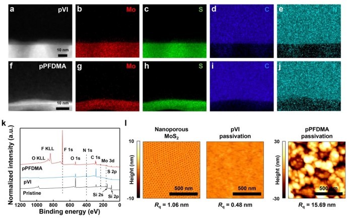
Figure 1 describes a process for fabricating nanoporous MoS2 using a multilayer MoS2 film transferred onto a Si/SiO2 substrate, followed by the selfassembly of a block copolymer layer to create a periodic nanohole pattern, and selective decomposition of the polymer block to obtain the desired nanoporous structure. The resulting nanoporous MoS2 was characterized using various analytical techniques, such as STEM, Raman spectroscopy, and XPS, which revealed its morphological and chemical properties. Polymeric passivation of nanoporous MoS2 Figure 2 shows a schematic of the polymer deposition process on the nanoporous MoS2 surface. The polymeric passivation layers, specifically pVI and pPFDMA are used on nanoporous MoS2 surfaces using the iCVD process. The process allows for solvent-free deposition at a low temperature, which minimizes damage to the substrate surface. The resulting polymer films preserve the chemical functionalities of the monomers and have distinct electrical properties. Raman spectroscopy and UPS analyses were performed to investigate the variation in the electrical characteristics of the nanoporous MoS2 films with each polymer passivation layer. The pVI passivation layer induced an n-doping effect, while the pPFDMA passivation layer induced an insignificant p-doping effect. The electrical effects of the two polymer layers were observed to be highly coherent on both nanoporous and non-patterned MoS2 films. Characterization of polymerpassivated nanoporous MoS2 film In figure 3, the study used high-angle annular dark-field (HAADF)-STEM analysis to confirm the effective passivation of two different polymer layers on nanoporous MoS2 . The crosssectional HAADF-STEM images with energy dispersive spectroscopy (EDS) mapping showed that both polymer layers were deposited conformally on the surface without notable defects.
The surface chemical composition of the polymer-passivated nanoporous MoS2 was investigated by XPS and compared with pristine nanoporous MoS2 , showing that the polymer passivation layer conformally covered the nanoporous MoS2 surface. To further investigate the surface properties of the polymer-passivated nanoporous MoS2 , AFM analysis was performed using a scanning probe microscope (XE-100, Park Systems). The AFM image of the pristine nanoporous MoS2 clearly exhibited porous structure and the smooth, amorphous surface morphology was confirmed with the root-mean-square roughness (Rq) < 0.5 nm, which also indicates that the pVI layer conformally covered the nanoporous MoS2 . On the other hand, the AFM image of the pPFDMA-passivated nanoporous MoS2 exhibited the roughened surface with the Rq value > 15 nm. This rough surface morphology was originated from the highly crystalline nature of pPFDMA due to the fluoroalkyl chain, which can also improve the hydrophobicity of the surface. The water contact angle (WCA) analysis also verified that the surface property of the nanoporous MoS2 was controlled according to the deposition of the polymer films (Supplementary Fig. 7). Therefore, it follows from the comprehensive analyses that the vapor-phase-deposited polymer passivation layers conformally covered the nanoporous MoS2 surface without incurring defect or damage to the underlying MoS2 , while fully retaining the chemical functionalities of each polymer film.

Figure 1: Fabrication and observation of nanoporous MoS2 film.
From: Functional polymeric passivation-led improvement of bias stress with long-term durability of edge-rich nanoporous MoS2 thin-film transistors.

Figure 2: Polymeric passivation of nanoporous MoS2 , films using pI and pPFDMA respectively.
From: Functional polymeric passivation-led improvement of bias stress with long-term durability of edge-rich nanoporous MoS2 thin-film transistors
Electrical characteristics of nanoporous MoS2 TFTs passivated by pVI and pPFDMA polymers
The study investigated the effect of passivation with pVI and pPFDMA layers on the electrical characteristics of nanoporous MoS2 TFTs, Figure 4. The passivation with both polymer layers effectively prevented charge trapping on the MoS2 edge-air interface and reduced hysteresis. The pVI layer induced n-doping behavior and a significant increase in the drain current (IDS), while the pPFDMA layer minimally changed the electrical characteristics of the TFTs. The polymer layers had little effect on the carrier scattering at the interface between the nanoporous MoS2 and the polymer. The output curves showed a more prominent increase IDS in the NANOscientific 12 magazine.nanoscientific.org lower range of gate voltage (VGS) for pVI-deposited TFTs and a practically identical shape for pPFDMA-deposited TFTs.

Figure 3: Chemical and morphological properties of polymer-passivated nanoporous MoS2 films.
From: Functional polymeric passivation-led improvement of bias stress with long-term durability of edge-rich nanoporous MoS2 thin-film transistors

Figure 4: Electrical properties of polymer-passivated nanoporous MoS2 TFTs.
From: Functional polymeric passivation-led improvement of bias stress with long-term durability of edge-rich nanoporous MoS2 thin-film transistors
Stability tests of pPFDMA-passivated nanoporous MoS2 TFTs
Figure 5 shows the passivation effect of the pPFDMA layer grown by iCVD on the nanoporous MoS2 TFTs. Gate-bias stress tests and long-term storage tests were conducted under ambient air conditions to examine the passivation performance of the pPFDMA layer on the nanoporous MoS2 TFTs. The results suggest that the pPFDMA passivation layer can effectively prevent the charge trapping induced by the adsorption of oxygen or water in an ambient environment at the edge defect sites. The long-term storage test also confirms the excellent passivation performance of the pPFDMA polymer synthesized by the iCVD process for robust nanoporous MoS2 devices.

Figure 5: Gate bias and illumination stress tests and long-term storage test of pPFDMA-passivated nanoporous MoS2 TFTs.
From: Functional polymeric passivation-led improvement of bias stress with long-term durability of edge-rich nanoporous MoS2 thin-film transistors
SUMMARY
In summary, the study demonstrates an efficient passivation method for nanoporous MoS2 using polymeric passivation layers via iCVD process. The proposed solvent-free method effectively passivated the surface edges and defects in nanoporous MoS2 , without damaging or degrading its structure and electrical integrity. The pVI with an electron-donating imidazole ring and pPFDMA containing a fluoroalkyl chain were utilized as n-doping and inert polymer passivation layers, respectively. Both polymer passivation layers conformally covered the underlying nanostructured MoS2 . The nanoporous MoS2 -based TFT with the polymer passivation layers showed a significant negative VTH shift in the pVI-deposited nanoporous MoS2 TFT, whereas the pPFDMA-deposited nanoporous MoS2 TFT only exhibited a small reduction in the on-current. On the other hand, the long fluoroalkyl chain in the pPFDMA provided strong hydrophobicity, thus remarkably enhancing the stability of the nanoporous MoS2 TFT in ambient air. The pPFDMA-deposited nanoporous MoS2 TFT demonstrated outstanding stability in the PBS, NBS, PBIS, and NBIS tests compared to the non-passivated device, primarily because the pPFDMA can efficiently abate the water and oxygen adsorption on the nanoporous MoS2 surface. In addition, only a negligible change was observed in the long-term storage test, which confirms the robustness of the pPFDMA-deposited nanoporous MoS2 TFT. The study provides an effective strategy for the passivation of nanostructured 2D materials. In particular, a vapor-phase deposited fluoropolymer can enhance the ambient stability of nanostructured 2D materials-based TFTs, without damaging their electrical characteristics.