How to tailor the crystallographic orientation evolution and surface morphological features of polycrystalline conductive N-type ZnO films
- 02 Jun 2023
- Volume 24
- NANOscientific Magazine, Spring 2023
Tetsuya Yamamoto, Research Institute, Kochi University of Technology, Japan
Introduction
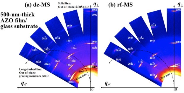
Highly transparent conductive oxide (TCO) films, such as n-type In2 O3 - and ZnO-based films, are of great interest for use as transparent conducting electrodes in optoelectronic devices (e.g., photovoltaic solar cells and flat display panels [1-4]). It is essential to adjust the trade-off between optical transparency and electrical conductivity to meet the requirements of various applications. Recently, atomic force microscopy (AFM: Park Systems NX10) has been used to analyze the data from a two-step film growth technique [5-8]. It has demonstrated to be an effective way of improving the electrical properties and tailoring the texture and surface morphology of transparent conductive Al-doped ZnO (AZO) polycrystalline films. Therefore, AZO films are a promising alternative to the commonly used Sn-doped In2 O3 (ITO), as Al and Zn are cheap, nontoxic and abundant raw materials. It is well known that the electrical and optical properties of polycrystalline AZO films strongly depend on filmgrowth methods. The conventional and representative film-growth methods are direct current (dc) magnetron sputtering (dc-MS) [9] or radio frequency (rf) MS (rf-MS) [9]. Although dc-MS has the advantage of higher film-growth rates over rf-MS from a production standpoint, there are still issues that need to be resolved. Rf-magnetron-sputtered AZO (rf-MS-AZO) polycrystalline films deposited on the amorphous glass substrates have a texture with a well-defined (0001) orientation (see Figure 1) [6,7]. On the other hand, polycrystalline AZO films deposited by dc-MS have a texture with a mixed orientation of the (0001) plane with other planes, such as (10-11), (20-21) and (30-32) (see Figure 1)) [6,7]. This leads to a large contribution of grain boundary (GB) scattering to carrier transport compared with rfMS-AZO polycrystalline films, resulting in a reduced Hall mobility (µH).

Figure 1. Out-of-plane wide-range reciprocal space maps (RSMs) of 500 nm-thick Al-doped ZnO (AZO) films on glass substrates deposited by (a) dc-MS and (b) rf-MS. q// and q1 represent the coordinates of the reciprocal space in the directions parallel and perpendicular to the surface, respectively.
The presence of the above GB in polycrystalline films reduces carrier transport, as evidenced by Hall effect measurements which show µH to be lower than the intrinsic carrier mobility in grains determined by optical measurements [10,11]. Additionally, dc-magnetron-sputtered AZO (dc-MS-AZO) films deposited on amorphous glass substrates have a high average roughness (Ra ) compared with rf-MS-AZO films deposited on amorphous glass substrates at any given film thickness, as seen in Figs. 2 and 3. In such films, lowered visible optical transmission are observed. To address these issues, we have developed a technology in which a 10 nm-thick rf-MS-AZO film, referred to as a critical layer, is inserted at the dc-MS-AZO film/substrate interface; It is essential that this critical layer has a feature of texture showing a preferential c-axis orientation on amorphous glass substrates.
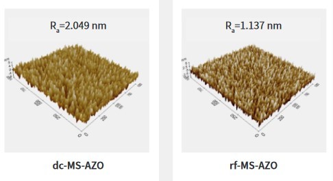
Figure 2. AFM images of (a) a 50 nm-thick dc-MS-AZO film on a glass substrate and (b) a 50 nm-thick rf-MS-AZO film on a glass substrate.
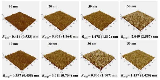
Figure 3. AFM images of AZO films of various thicknesses deposited on amorphous glass substrates by dc-MS (upper part) and rf-MS (lower part).
Experimental
We deposited AZO films on amorphous glass substrates (Corning Eagle XG) at a substrate temperature of 200 °C using MS apparatus (ULVAC CS-L) with a dc or rf power of 200 W. The oxide targets (Toshima Manufacturing Corp.) were high-density sintered circular AZO targets (diameter: 80 mm) with an Al2 O3 content of 2.0 wt. % (3.16 mol.%). To investigate the effects of the critical layer on the surface and electrical properties of dc-MS-AZO films deposited on amorphous glass substrates, four types of samples were prepared [7]. Sample 1 was a 500 nm-thick rf-MS-AZO film on an amorphous glass substrate; sample 2 was a 500 nm-thick dc-MS-AZO film on the glass substrate; for sample 3, we first a 10 nm-thick rf-MS AZO film on the glass substrate as the critical layer, followed by a 490 nm-thick dc-MS AZO film; for sample 4, we first deposited a 10 nm-thick dc-MS-AZO film on the glass substrate as the critical layer, on which we subsequently deposited a 490 nmthick rf-MS-AZO film. The temperature of the amorphous glass substrate was fixed at 200 °C for all deposition processes of samples. For a comprehensive analysis of the textures of the thick AZO films, we conducted out-of-plane widerange reciprocal space maps (RSMs) measurements using a SmartLab XRD system (Rigaku Corp.) equipped with a PILATUS 100K/R two-dimensional X-ray detector and Cu Kα̅ radiation (wavelength λ = 0.15418 nm, based on the weighted average of Cu Kα1 (λ = 0.154059 nm) and Cu Kα2 (λ = 0.15444 nm) in an intensity ratio of 2:1) [12]. The surface morphology was analyzed by AFM (Park Systems NX10) [13], with a scan area and speed of 1×1 µm2 and 2 µm/s (1 Hz scan rate), respectively. Ra , root-mean-square roughness (Rq ) and surface kurtosis (Rku) were used to evaluate the surface morphology of the AZO films deposited directly on the glass substrates or on the glass substrates with the critical layer. The electrical properties, carrier concentration (ne ), µH and electrical resistivity (ρ), were determined at room temperature by Hall effect measurements in a van der Pauw geometry (Nanometrics, HL5500PC).
Results and Discussion
Figure 3 displays AFM images of AZO films with various thicknesses deposited on amorphous glass substrates by dc-MS (upper part) and rf-MS (lower part). In Figure 3, we indicate Rq and Ra in all the films. The ratio of Rq to Ra is almost 1.25 for rf-MS-AZO films with thicknesses of more than 20 nm [7], indicating that such films have surfaces with a Gaussian height distribution (theoretical value is sqrt(pi/2)) [14,15]. 10 nm-thick dc-MS and rf-MS-AZO films had Rku of more than 3, which suggests a spikey surface with a large number of high peaks and low valleys [14]. The rf-MS-AZO films with thicknesses of 20 nm or more had Rku of 3, which indicates a perfectly random surface [14]. On the other hand, for dc-MS-AZO films, Rku was below 3 regardless of the thickness, suggesting a bumpy surface with few high peaks and low valleys. This can prevent the lateral growth caused by the sufficient migration of adatoms such as Zn, Al and O atoms from one grain to adjacent grains; bumps located at higher surface positions may grow faster at the expense of other valleys, leading to the enhanced surface roughness shown in Figure 3. In such films, poor additional lateral relaxation processes during film growth will inevitably cause dynamic roughening, i.e., the surface roughness increases as the thickness increases (see Figure 4). Figure 4 shows Rq of AZO films with thicknesses ranging from 10 to 50 nm deposited on amorphous glass substrates by dc-MS or rf-MS. It is evident that Rq of dc-MS-AZO films show a sharp increase compared with rf-MS-AZO films with increasing the film thickness.
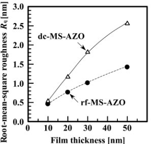
Figure 4. Root-mean-square roughness (Rq ) of AZO films with thicknesses ranging from 10 to 50 nm deposited on amorphous glass substrates by dc-MS or rf-MS.
In Table 1, we summarized the surface properties and lateral grain sizes calculated using the data determined from in-plane XRD measurements of each sample. Figure 5 shows cross-sectional schematic diagrams, AFM images and out-of-plane wide-range RSMs of samples 2 and 3. The results in Figure 5 and Table 1 demonstrate that the use of 10 nm-thick critical layers composed of rfMS-AZO films deposited on amorphous glass substrates drastically reduced Ra and Rq of 490 nm-thick dc-MSAZO films grown on the critical layers (sample 3) compared with those of the dc-MS-AZO Ra =2.049 nm Ra =1.137 nm rf-MS-AZO magazine.nanoscientific.org NANOscientific 15 other samples, particularly 500 nm-thick dc-MS-AZO films deposited on amorphous glass substrates (sample 2). The top and bottom out-of-plane wide-range RSMs in Figure 5 demonstrate that the postannealing-free technology using only very thin critical layers yields thick dc-MS-AZO films with a texture featuring a well-defined (0001) crystallographic orientation between columnar grains, resulting in the formation of small-angle grain boundaries. This leads to an increase in ne by 6.76 % and µH by 15 % compared with thick AZO films deposited on critical-layer-free glass substrates, resulting in a decrease in ρ, which is inversely proportional to the product of ne and µH, by 18.3 % (ρ =2.32×10⁻⁴ Ωcm). The improvement of µH is attributed to the fact that the GB scattering mechanism contributes very little to the carrier transport.
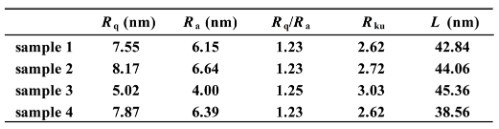
Table 1. Root-mean-square roughness (Rq ), average roughness (Ra ), ratio (Rq / Ra ) of Rq to Ra , surface kurtosis (Rku) and lateral grain size (L) of Samples 1-4. See text (Experimental section) for details of each sample.
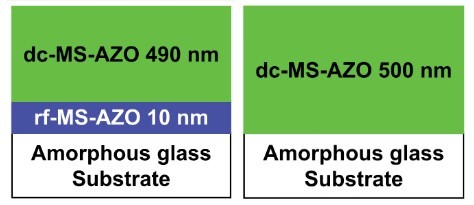
Figure 5. Cross-sectional schematic diagrams, AFM images and out-ofplane wide-range RSMs of sample 3 (upper part) and sample 2 (lower part).
Conclusion
By analyzing the experimental data of the surface morphology and crystallographic orientation distribution of rf- and dcmagnetron-sputtered AZO films of various thicknesses deposited on amorphous glass substrates, we developed a two-step deposition technique using a 10 nm-thick AZO-based critical layer to produce dc-MS-AZO films with a texture that has a preferential c-axis orientation perpendicular to the substrates and a significantly improved surface morphology. The combined results of AFM and XRD provided a comprehensive understanding of key factors governing the crystallographic orientation evolution and surface morphological features in polycrystalline AZO films. Such knowledge can be used to develop the deposition process and conditions to achieve the desired surface morphologies and electrical properties for optoelectronic device applications.
References
1. Z. M. Jarzebski, Preparation and physical properties of transparent conducting oxide films, Phys. Status Solidi. 71 (1982) 13–41.
2. K. L. Chopra, S. Major, D. K. Pandya, Transparent conductors-A status review, Thin Solid Films 102 (1983) 1–46.
3. P. P. Edwards, A. Porch, M. O. Jones, D. V. Morgan, R. M. Perks, Basic material physics of transparent conducting oxides, Dalton Trans. 19 (2004) 2995–3002.
4. N. Yamamoto, H. Makino, S. Osone, A. Ujihara, T. Ito, H. Hokari, T. Maruyama, T. Yamamoto, Development of Ga-doped ZnO transparent electrodes for liquid crystal display panels, Thin Solid Films, 520 (2012) 4131–4138.
5. J. Nomoto, H. Makino, T. Yamamoto, High-Hall-mobility Al-doped ZnO films having textured polycrystalline structure with a well-defined (0001) orientation, Nanoscale Res. Lett. (2016) 11:320.
6. J. Nomoto, K. Inaba, M. Osada, S. Kobayashi, H. Makino, T. Yamamoto, Highly (0001)-oriented Al-doped ZnO polycrystalline films on amorphous glass substrates, J. Appl. Phys. 120 (2016) 125302–1–125302–11.
7. J. Nomoto, K. Inaba, S. Kobayashi, H. Makino, T. Yamamoto, Interface layer to tailor the texture and surface morphology of Al-doped ZnO polycrystalline films on glass substrates, J. Cryst. Growth 468 (2017) 645–649.
8. J. Nomoto, H. Makino, T. Nakajima, T. Tsuchiya, T. Yamamoto, Improvement of the Properties of Direct-Current Magnetron-Sputtered Al-Doped ZnO Polycrystalline Films Containing Retained Ar Atoms Using 10-nm-Thick Buffer Layers, ACS Omega 4 (2019) 14526–15536.
9. T. Minami, New n-Type Transparent Conducting Oxides, MRS Bulletin 25 (2000) 38–44.
10. H. Fujiwara, M. Kondo, Effects of carrier concentration on the dielectric function of ZnO:Ga and In2O3:Sn studied by spectroscopic ellipsometry: Analysis of free-carrier and band-edge absorption, Phys. Rev. B 71 (2005) 075109–1–0751090–10.
11. T. Yamada, H. Makino, N. Yamamoto, T. Yamamoto, Ingrain and grain boundary scattering effects on electron mobility of transparent conducting polycrystalline Ga-doped ZnO films, J. Appl. Phys. 107 (2010) 123534–1–123534–8.
12. S. Kobayashi, K. Inaba, X-ray thin-film measurement techniques VIII. Detectors and series summary, Rigaku J. 28 (2012) 8–13.
13. https://parksystems.com/products/small-sample-afm/park-nx10/overview
14. H. C. Ward, Rough Surfaces, T. R. Thomas Ed., Longman, London cop. (1982).
15. B. R. Kumar, T. S. Rao, AFM studies on surface morphology, topography and texture of nanostructured zinc aluminum oxide thin films, Dig. J. Nanometer. Bios. 7 (2012) 1881–1889.