Semiconductor Spintronics: Electrical Spin Injection and Transport in Semiconductors: Fabrication and Development of Prototype Spintronic Devices
- 17 Mar 2017
- Volume 9
- NanoScientific Magazine, Winter 2017

Senior Scientist and Head of the Magnetoelectronic Materials & Devices section in the Materials Science & Technology Divison at the Naval Research Laboratory, Washington, DC
Dr. Jonker’s is recognized industry-wide for his exemplary career achievements including his work in electron spin. He has been integral in developing solutions for key problems and demonstrating essential enabling steps in utilization of electron spin as an alternate state variable for information storage and processing in semiconductors, including electrical spin injection, detection and generation of pure spin currents. His research has also provided significant advances in the fundamental science of magnetoelectronics, particularly in interfacing the two dominant materials technologies of information storage and processing: that of ferromagnetic metals (magnetic storage) and semiconductors (logic, processing). This has led to results that enable the development of future spin-based electronics that are faster, instant-on, non-volatile with higher functionality and lower power consumption than existing charge-based electronics, that will advance capabilities of Navy / Marine Corps platforms of the "Navy after next." He is at the center of multidisciplinary research efforts, providing scientific leadership and vision to develop magnetoelectronic materials and technologies for information sensing, processing and storage including the initiation and coordination of several large research programs from 2007 to 2010 totaling ~ $15 million. He is a key advisor on science/technology problems of extraordinary scope and a panel member and contributing author for International Technology Roadmap for Semiconductors, as well as an advisor on strategic research planning for the Office of Naval Research, the Defense Advanced Research Projects Agency, the National Science Foundation and the Army Research Office.
"WE SELECTED THE PARK NX 10 AFM INSTRUMENT ON A COST/ PERFORMANCE RATIO BASED ON OUR BID SPECIFICATIONS. THE SPECIALIZED SCIENTIFIC INSTRUMENT EQUIPMENT MARKET IS AN INTERNATIONAL MARKET, WE EVALUATED A NUMBER OF COMPANIES WORLD-WIDE BEFORE SELECTING PARK SYSTEMS AFM. PARK SYSTEMS AFM WAS IDENTIFIED AS THE ONE THAT WOULD GET THE HIGHEST RETURN FOR THE COST OF PURCHASE.”
What are Magnetoelectronic devices and how are you using them?
My current work involves looking at materials properties and how they interface including magnetic metals. Select materials promise to be thero magnetic meaning they have a non zero phenomenon or a magnetic moment. This is used universally in motors, tools, etc. We are currently looking at developing material for IT non volitale memory for reprogramming logic, ultra low power consumption for devices and circuits and sensors for drones. These will allow us to leave a device underwater or for it to be taken out into field without carrying batteries. We are focusing on ultra low power consumption devices we can leave anywhere or have delivered by drones.
How do you use microscopy in your research?
Sensors cover a broad area for sonar optical and magnetic sensors. We routinely use SEM, AFM, MFM, and a variety of optical spectroscopy to evaluate materials we grow. We do a lot of material synthesis and have a broad suite of characterization tools. The Park NX 10 AFM is one of our tools. It was selected in our government procurement program largely due to the cost performance ratio based on our bid specifications and was used in recent research published in ACS Omega on the first demonstration of metallic spin. This offers exciting opportunities for the advancement of sensors and data storage. Specialized scientific equipment market is an international global market. Our laboratory has a wide array of equipment for measurement including spin-polarized scanning tunneling microscopy (STM) and many others pieces of the most modern equipment available world-wide.
NRL PRODUCES SPIN FILTERING AT ROOM TEMPERATURE WITH GRAPHENE
An interdisciplinary team of scientists at the U.S. Naval Research Laboratory (NRL) have reported the first demonstration of metallic spin filtering at room temperature using ferromagnet-graphene-ferromagnet thin film junction devices — spin is a fundamental property of electrons, in addition to charge, that can be used to transmit, process and store data. “The spin filtering had been theoretically predicted and previously seen only for high-resistance structures at cryogenic temperatures,” said Dr. Enrique Cobas, principal investigator, NRL Materials Science and Technology Division. “The new results confirm the effect works at room temperature with very low resistance in arrays of multiple devices.” The thin film junctions demonstrated low resistance, and the magnetoresistance characteristic of a spin filter interface from cryogenic temperatures to room temperature. The research team also developed a device model to incorporate the predicted spin filtering by explicitly treating a metallic minority spin channel with spin current conversion, and determined that the spin polarization was at least 80 percent in the graphene layer. “Graphene is famous for its extraordinary in-plane properties, but we wanted to look at conductivity between stacked graphene sheets and how they interact with other materials,” said Cobas. To do so, NRL researchers developed a recipe to grow large multi-layer graphene films directly on a smooth, crystalline nickel alloy film while retaining that film’s magnetic properties, then patterned the film into arrays of cross-bar junctions. “We also wanted to show we could produce these devices with standard industry tools, not just make one device,” Cobas added. The spin filtering phenomenon is due to an interaction of the quantum mechanical properties of graphene with those of a crystalline nickel film. When the nickel and graphene structures align, only electrons with one spin can pass easily from one material to the other, an effect termed spin filtering, that results in spin polarization of an electric current. “There is room for improvement as theory suggests the effect can be increased by an order of magnitude by fine-tuning the number of graphene layers,” said Dr. Olaf van ‘t Erve, research scientist, NRL Materials Science and Technology Division. “However, current models do not include the spin-conversion that happens inside the ferromagnetic contacts. Once we account for those effects, we’re already close to the ideal case of 100 percent spin polarization in the graphene layer, enabling us to revise our device geometry and materials to maximize the effect.”

Conceptual rendering of a spin-filtering graphene junction: Films of nickel (shown in blue) and iron (shown in red) contain a mixture of electrons with up and down spins. A few layers of graphene (shown in grey) lie between the metal layers to create a conductive path for electrons of one spin only, while blocking the other spin. A current driven though the metallic junction (labeled as 'J') becomes spin polarized. (U.S. Naval Research Laboratory)
The result is relevant to next-generation nonvolatile magnetic random access memory (MRAM), which uses spin-polarized pulses to flip a magnetic bit from 0 to 1 and viceversa. It may also find use in future spin logic technologies or as magnetic sensors. The research results are reported in the November 2, 2016, issue of ACS Nano (DOI 10.1021/acsnano.6b06092). The full research team included Drs. Enrique Cobas, Olaf van ‘t Erve, Shu-Fan Cheng, Konrad Bussman and Berry Jonker from the Materials Science and Technology Division and Drs. James Culbertson and Glenn Jernigan from the Electronics Science and Technology Division at NRL.

Spatial Control of Photoluminescence at Room Temperature by Ferroelectric Domains in Monolayer WS2/PZT Hybrid Structures Connie H. Li, Kathleen M. McCreary, and Berend T. Jonker Materials Science and Technology Division, Naval Research Laboratory Supporting Information.
ABSTRACT: Single-monolayer transition metal dichalcogenides exhibit exceptionally strong photoluminescence (PL), dominated by a combination of distinct neutral and charged exciton contributions. We show here that the surface charge associated with ferroelectric domains patterned into a lead zirconium titanate film with an atomic force microscope laterally controls the spatial distribution of neutral and charged exciton populations in an adjacent WS2 monolayer. This is manifested by the intensity and spectral composition of the PL measured in air at room temperature from the areas of WS2 over a ferroelectric domain with a polarization dipole pointed either out of the surface plane or into the surface plane. This approach enables spatial modulation of PL intensity and trion/ neutral exciton populations and fabrication of lateral quantum dot arrays in any geometry, with potential applications in nonvolatile optically addressable memory or optical quantum computation.
See complete article at: http://pubs.acs.org/journal/acsodf
“THE POTENTIAL APPLICATIONS WOULD CERTAINLY BE LONG-TERM, BECAUSE SO LITTLE IS KNOWN AT THIS POINT, EXPLAINS NRL’S DR. BERRY JONKER. THE EXISTENCE OF THIS NEW QUANTUM PHASE OF MATTER WAS JUST CONFIRMED IN 2008 AND ITS PROPERTIES YET TO BE FULLY UNDERSTOOD, SO IT IS A BIT DIFFICULT TO SPECULATE ON APPLICATIONS. BUT POTENTIAL APPLICATION AREAS INCLUDE RECONFIGURABLE ELECTRONICS, SPINTRONICS AND QUANTUM INFORMATION PROCESSING.” DR. BEREND T. JONKER

The Honorable Robert Work, Under Secretary of the Navy, presents the Presidential Rank Award to NRL's Dr. Berend Jonker. (Photo: U.S.Naval Research Laboratory, Jamie Hartman)
In 2011, Dr. Berend Jonker, Senior Scientist for Magnetoelectronics at the Naval Research Laboratory, was the recipient of the Presidential Rank Award for Meritorious Senior Professional, recognizing Dr. Jonker for leading long-term basic research in developing magnetoelectronic materials and technologies, and demonstrating prototype device concepts that offer increased performance for information sensing, processing and storage for supporting the Navy/Marine Corps of tomorrow and the global war on terrorism.

The NRL research team, left to right: Dr. Berend Jonker, Dr. Jeremy Robinson, Dr. Connie Li, and Dr. Olaf van’t Erve. (Photo: U.S. Naval Research Laboratory
In 2014, the NRL research team above demonstrated for the first time that one can electrically access the remarkable properties predicted for a topological insulator (TI). This accomplishment identifies a successful electrical approach that provides direct access to the TI surface state spin system, significantly advances our fundamental understanding of this new quantum state, and enables utilization of the remarkable properties these materials offer for future technological applications.

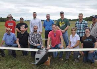
Members of the chemistry and tactical electronic warfare divisions from the U.S. Naval Research Laboratory with the Ion Tiger unmanned air vehicle, which recently flew with a new, custom hydrogen fuel cell designed and built at NRL. The fuel cell system is capable of 5,000 watts and is made of formed and laser-welded metal foil bipolar plates, which saves space and weight. “NRL having the know how to build their own fuel cells in house gives the U.S. Navy the understanding and tools needed for transitioning fuel cells to the fleet,” said Michele Anderson, program manager at the Office of Naval Research.