Scanning Capacitance Microscopy Characterization of VacuumChannel Nanoelectronic Devices
- 17 Mar 2017
- Volume 9
- NanoScientific Magazine, Winter 2017
G. Pascual1 , B. Kim1 , and K. Lee1 1 Park Systems Inc., 3040 Olcott Street, Santa Clara, CA 95054, United States of America J.W. Han2 2 NASA Ames Research Center, Moffett Field, CA 94035, United States of America
ABSTRACT
Efforts to harden electronic components and systems using solid-state devices against the effects of radiation and heat for use in space travel have become a major engineering operation for space exploration agencies around the world. Such work has not only been time-consuming, but expensive as well with the majority of deliverable solutions being costlier and technologically older than what is typically available to consumers for other types of application. To address the drawbacks of using solid-state devices in space, research has begun focusing on reviving vacuum tube technology using silicon-based fabrication models as an alternative solution. In this investigation, a newly developed vacuum-channel nanoelectronic device was characterized via scanning capacitance microscopy (SCM) using a Park NX20 atomic force microscopy (AFM) system to assess its viability as a transistor. The representative sample had its source-drain interface examined using a scan area of 450 x 800 nm. The capacitance data acquired reveals the device may be electrically viable as a functional transistor. Its source and drain were each observed to have an average capacitance (represented in units of voltage) of -1.4 μV while the circular dots next to the end of each terminal exhibited an average capacitance of -1.8 μV. The region of the vacuum-channel between the aforementioned dots was observed to have the most positive relative capacitance amongst all features in the scan area with an average recorded value of 2.3 μV.
INTRODUCTION
From their invention at the beginning of the 20th century, vacuum tubes were used as basic electronics components that enabled the proliferation of devices which have had an incalculable impact on human society: television and radio, telephone networks, industrial process controls, and more. However, vacuum tube-based electronics were eventually rendered outmoded by the advent of solid-state devices powered by semiconductor devices. By mid-century, semiconductor devices, with their smaller footprint, greater efficiency, longer longevity, and lower cost, became the de facto wellspring for mass-produced electronics and would eventually grow into the multi-billion dollar industry it is today. However, with humanity now more than a decade into the 21st century, the challenge of expanding our space exploration efforts has revealed that semiconductor devices are vulnerable to the types of radiation that bombard spaceborne equipment. Efforts to harden components and systems have become a major engineering operation for space exploration agencies [1] and other organizations that seek to safeguard their electronic components and systems. Unfortunately, such processes are not only time-consuming but expensive; hardening electronics against radiation and heat lead to solutions that are both costlier and older than what is available to other types of consumers [2].
In order to address these drawbacks and produce a transistor technology that can achieve higher speeds and frequencies than any semiconductor device, research has begun focusing on reviving vacuum tube technology and applying its principles at nanoscale whilst still leveraging a silicon-based fabrication method. The result is a vacuum-channel transistor device which could potentially be manufactured at an industrial scale using already existing silicon fabs for solid-state transistor devices [2]. This investigation uses Scanning Capacitance Microscopy (SCM) to investigate the nanoscale electrical properties of a newly developed vacuum-channel device to both ascertain its viability as a transistor as well as to observe if the method used to fabricate its gate insulators can be controlled.
METHODOLOGY
To acquire data regarding the vacuum-channel device’s nanoscale electrical properties, a Park NX20 Atomic Force Microscopy (AFM) system was used to run SCM scans of the device area containing the source-drain interface, vacuum channel, and insulated gates. Supplemental topographical data at the scan area was collected simultaneously through contact mode AFM using the same probe.
SCM with AFM
SCM with AFM is a powerful combination for investigating transistor devices—together, the two methods provide the user with a nondestructive process of characterizing both charge distribution and surface topography with high spatial resolution and sensitivity [3]. In SCM, a metal probe tip and a highly sensitive capacitance sensor augment standard AFM hardware. A voltage then is applied between the probe tip and the sample surface creating a pair of capacitors in series (in Metal-OxideSemiconductor devices) from (1) the insulating oxide layer on the device surface and (2) the active depletion layer at the interfacial area between the oxide layer and doped silicon. Total capacitance is then determined by the thicknesses of the oxide layer as well as the depletion layer which is influenced by the both how doped the silicon substrate is well as the amount of DC voltage being applied between the tip and device surface.

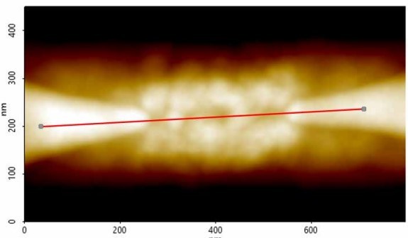
Figure 1. Contact mode AFM topography image of the vacuum-channel device’s source-drain interface. The overlaid red line corresponds to the topography line profile displayed in Figure 2. Scan size: 450 x 800 nm
The principle of how capacitance is measured in vacuum-channel devices via SCM is similar. Again, a thin layer of oxide is used as insulation on the device [4], this time insulating the gate from the source-drain interface on the device surface. A DC voltage is applied between the probe tip and the sample surface as the tip scans across various device features. The data of the detected changes in capacitance are also supplemented by AFM data generated by recording the deflections of the probe’s cantilever as the tip engages the device surface [5]. As the sample scan is being completed, a laser beam is reflected off the probe cantilever and onto a position-sensitive photodiode. The deviations of the laser’s position are then processed with software to create a rendering of the device’s surface topography.
RESULTS AND DISCUSSION
Device Topography
The vacuum-channel device (Device 4) was scanned at an area measuring 450 x 800 nm capturing its source-drain interface. Contact mode AFM reveals that the source and drain terminals are shaped into sharp tips. This design was implemented in order to intensify the electrical field generated at this location [4]. The topography data at this location also reveals the distance between the source and drain tips, a span which includes Device 4’s the ends of the source-drain terminals and enclosed vacuum-channel, is approximately 250 nm (Figure 1). For reference, the mean free path of electrons and gas molecules under normal atmospheric pressure is about 200 nm [2]. If the voltages running through the device were kept low enough, the electrons traversing from source to drain would not have energy to ionize any lingering gas molecules left in the channel [4]. Therefore, Device 4 could technically operate without incident under normal air pressure—the presence of a vacuum in the channel serves as an extra precaution to guard against ionized molecules from damaging the terminals of the sourcedrain interface. Inspection of the topography line profile (Figure 2) for this image reveals the distance from the tallest peaks to the lowest valleys in this vacuum-channel are in excess of 5 nm. Of further interest are two bumps, speculated to be the device’s quantum dots, which represent the peak heights in the vacuum-channel and stand on either end of the span in close proximity to the end of each terminal.

Figure 2. Line profiles of the AFM topography (red, left y-axis in nm) and the capacitance data (green, right y-axis in μV) of the device area scanned in Figures 1 and 3.
Device Capacitance with Topography
SCM data from was also gathered from the same 450 x 800 nm scan discussed above. This image (Figure 3) shows each of Device 4’s source-drain terminals being darker in color, or more negatively charged, than other portions of the device. Note the difference in color of the terminals and nearby suspected quantum dots—these features are both more negatively charged than the rest of the imaged area. This is corroborated by the capacitance line profile (Figure 2) which shows an average capacitance (represented in units of voltage) of about -1.4μV in areas corresponding to the device’s source and drain terminals. Of further significant note is the even slightly more negative -1.8 μVvalues recorded in areas corresponding to the quantum dots adjacent to the ends of each terminal.
Another important feature clearly seen in the capacitance image is the portion of Device 4’s vacuum-channel between each of the quantum dots. This area shows a brighter, more positively charged region with capacitance values as high as 2 μV being detected. This particular region, approximately 175 nm in length, cannot be easily identified in the topography image but is easily spotted with the greater contrast provided in the SCM image. The capacitance change from the suspected quantum dots standing adjacent to each source-drain terminal to the middle of the vacuum-channel is observed to be 3.8μV, the greatest change observed along the selected line profile.

Figure 3. An SCM capacitance image of the region containing the device’s source-drain interface. Brighter colors correspond to relatively more positively charged areas on the device whereas darker colors correspond to relatively more negatively charged areas. The overlaid green line corresponds to the capacitance line profile displayed in Figure 2. Scan size: 450 x 800 nm.
CONCLUSION
SCM together with AFM successfully characterized both the spatial variations in capacitance as well as the topography of a newly developedvacuum-channel nanodevice. By examining the line profiles of the topography and capacitance data acquired down an identical path on the device’s source-drain interface, additional insight was gained into the relationship ofkey physical structures with changes in capacitance. The device’s topography at its source-drain interface was imaged and revealed a vacuum-channel spanning 250 nm in length with peaks and valleys separated by a distance of approximately 5 nm. The electrical functionality of the device was assessed through the acquisition of a capacitance map. This map revealed a relatively negatively charged (-1.4 to -1.8μV) source-drain terminal and adjacent quantum dot followed by a relatively positively charged vacuum-channel (2μV) and another dot-terminalstructure (-1.4 to -1.8μV) on the other end of the source-drain interface. This alternating series of capacitance changes at these key structures suggest the device is capable of effective functionality as a transistor.
REFERENCES
1. A.S. Keys and M.D. Watson, Radiation Hardened Electronics for Extreme Environments, Huntsville, AL: NASA Marshall Space Flight Center, 2007.
2. Vacuum Nanoelectronics: Interview with M. Meyyappan and Jin Woo Han, EEWeb, 2013. Retrieved from https://www.eeweb.com/ blog/eeweb/interview-with-m.-meyyappan-and-jin-woo-han-onvacuum-nanoelectronics
3. Scanning Capacitance Microscopy (SCM), Park Systems, 2016. Retrieved from http://www.parkafm.com/index.php/park- spm-modes/94-electricalproperties/235-scanning-capacitance-microscopy-scm
4. J.W. Han and M. Meyyappan, Introducing the Vacuum Transistor: A Device Made of Nothing, IEEE Spectrum, 2014. Retrieved from http://spectrum.ieee.org/semiconductors/devices/introducing-the-vacuumtransistor-a-device made-of-nothing
5. How AFM Works, Park Systems, 2016. Retrieved from http://www.parkafm.com/index.php/medias/nano-academy/how-afm-works
KEYWORDS
AFM, atomic force microscopy, capacitance, characterization, scanning capacitance microscopy, SCM, semiconductor, silicon, topography, transistor, vacuum, vacuum-channel