Glimpses of the Nanoscale
- 26 Sep 2016
- Volume 8
- NanoScientific Magazine, Fall 2016
By Park Systems Staff
In our ongoing quest to understand and master the world around us, researchers from various fields have turned to looking at the world at nanometer resolution. Investigations at these dimensions can no longer be performed diffraction-limited tools such as optical microscopes. As a result, AFM and other Scanning Probe MIcroscopy techniques have become very attractive options to determine not just the topology of a sample, but also to explore various other properties as well.

High-resolution magnetic property image of hard disk drive media Scan area: 5 x 5 µm Probe: PPP-MFMR Technique: Magnetic Force Microscopy (MFM)

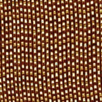
Topography of a bacterial S-layer membrane in liquid Scan area: 500 x 500 nm Technique: Atomic Force Microscopy (AFM)
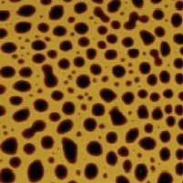
Phase image of lubricant on a plastic board Scan area: 30 x 30 µm Technique: Atomic Force Microscopy (AFM)
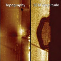
Topography of a FET structure vs. its dopant structure; the brightness in the SCM amplitude image correlates to dopant concentration in this part of the device Technique: Scanning Capacitance Microscopy (SCM)
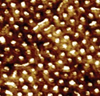
Topography of a block copolymer Scan area: 0.5 x 0.5 µm Probe: SSS-NCHR Technique: Atomic Force Microscopy (AFM)
In our ongoing quest to understand and master the world around us, researchers from various fields have turned to looking at the world at nanometer resolution. Investigations at these dimensions can no longer be performed diffraction-limited tools such as optical microscopes. As a result, AFM and other Scanning Probe MIcroscopy techniques have become very attractive options to determine not just the topology of a sample, but also to explore various other properties as well.
SPM techniques such as Scanning Ion Conductance Microscopy and AFM have been used to investigate biological matter such as cellular membranes under in-situ, liquid conditions. AFM has also been instrumental in novel polymer development such as the furthering of our knowledge of lubrication performance in tribology studies as well as the fabrication of higher-performance photoresist materials for wafer production. Inroads have also been made in the hard disk drive sector with the myriad nanoscale magnetic traits of a disk slider now openly characterized and ready for optimization by design engineers. Similar stories can be found again in the semiconductor industry—Scanning Capacitance Microscopy (SCM) is an extremely effective technique to verify the dopant concentration in new device designs. Dopant concentration is a materials property that cannot be gauged using topography data and can only be measured using SCM.