Park Systems Joins Forces with Imec to Develop Advancements in Nanoscale AFM Metrology Solutions for Semiconductor Manufacturing
- 01 May 2015
- Volume 4
- NanoScientific Magazine, Spring 2015

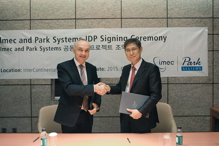
Dr. Luc Van den hove (President & CEO, Imec) and Dr. Sang-il Park (Chairman & CEO, Park Systems)

Park Systems has officially joined imec’s Industrial Affiliation Program (IIAP) and become a new member of IIAP at a signing ceremony in Seoul Korea on Feb 3, 2015. Park Systems is a world-leader in Atomic Force Microscopes (AFM) and signed a Joint Development Project (JDP) with nanoelectronics research center imec, to develop in-line AFM metrology solutions of future technology nodes including but not limited to surface roughness, thickness, critical dimension (CD), and sidewall roughness. The JDP will develop new protocol designed to increase production yield and device performance for the semiconductor industry. The partnership will develop a broad range of AFM metrology solutions for process development, production, and failure analysis. For surface roughness, the most accurate surface roughness measurement with wafer mapping and incoming material monitoring could be delivered. For thickness, accurate thickness value in pre- and post-processing will be delivered in order to complement the existing ellipsometry solution. More importantly, the partnership will explore a new frontier of high resolution 3D AFM FEATURE STORY Dr. Luc Van den hove (President & CEO, Imec) and Dr. Sang-il Park (Chairman & CEO, Park Systems) metrology to address accurate CD, line width roughness (LWR), line edge roughness (LER) measurements, and sidewall roughness during etch, EPI, film deposition, and lithography processes.
The JDP between Park Systems and imec will develop new in-line monitoring and analysis methods for semiconductor manufacturers as well as new production protocol for better process development and control, which will result in improved device performance and production yield. For example, the high resolution sidewall information on vertical planar and cylindrical structure by Park's new 3D AFM will bring huge impact on the performance of vertical devices such as FinFET, TFET, STT-MRAM and others.
As the design rule of semiconductor device shrinks, the CD measurement and sidewall variation in LER/LWR measurements became important and directly correlated with the leakage, hence device performance. CD-SEM, TEM, and OCD have been used for the CD metrology, but each technique has its shortcomings such as resolution and e-beam damage for CD-SEM, sample preparation and sample damage for TEM, and time-consuming process development for OCD. Now, the AFM enabled hybrid metrology is on the rise as the next generation in-line monitoring and analysis method of non-destructive CD control.
In the most recent decade, the predictive power and correlation of the new hybrid metrology saw a vast improvement, and Park's new 3D AFM metrology will contribute the detailed sidewall and nanoscale surface information for the critical components in the yield control matrix. The collaboration between Park Systems and imec will create an information gathering platform from a multi disciplinary team of leading experts of scientists, engineers, and researchers to work together to create the next generation solutions in semiconductor metrology.

“We are Grateful for the Opportunity to Partner with Imec in a Joint Development Project,” Comments Dr. Sang-il Park, CEO Of Park Systems. “This Partnership Between Park Systems and Imec Provides a Crucial Link of Scientific Collaboration Throughout the Chain of Suppliers and Vendors in Semiconductor Wafer Production. Significant Future Technological Advances will be Made From this JDP for Afmbased Inline Nanoscale Metrology.”
Imec’S Primary Focus Is On Research Programs That Improve Sustainability For Our Planet

Imec reported revenue (P&L) totaled 363 million euro in 2014 and their huge investment in nanoelectronics research is geared towards providing products and services for several industries. Their business model focuses on advanced scientific knowledge and an extensive base of global partnerships spanning a world-wide network of key contributors in top industries including ICT, healthcare and energy. Headquartered in Leuven, Belgium, with offices in Belgium, the Netherlands, Taiwan, USA, China, India and Japan, imec has a staff of about 2,200 people including almost 700 industrial residents and guest researchers.
The new technologies under development is developing will be the backbone of a number of solutions that will make the world a better, more sustainable place.
In life sciences, they will allow for a sustainable healthcare for more people. In communication, they will allow us to cope with the exponential growth in data and required computation. Energy solutions will mitigate our dependence on fossil fuels. Mobility solutions will make cities safer and more comfortable to live in.
But at the same time, the era of easy technology scaling is now far behind us. Every new technology node is becoming more complex and costly to develop. As a result, the R&D challenges and the required R&D budgets for the semiconductor industry keep growing year over year.