NANOscientific
Symposium Korea 2026
20 - 21 August, 2026 | Park Systems HQ, Gwacheon, South Korea
등록
개회 및 환영사
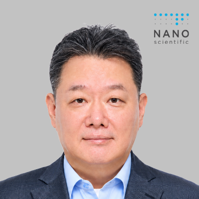
기조강연: 반도체 기술의 트랜드와 MI 기술의 방향
Semiconductor technology is now moving beyond the era of two-dimensional (2D) structures into the age of three-dimensional (3D) devices. While 2D development continues, the transition to 3D has significantly increased the complexity of research and development, requiring greater time and resources. To enhance device performance efficiently, extensive efforts are being made in co-optimization approaches such as DTCO and STCO.
Artificial Intelligence (AI) and Deep Learning (DL), which have recently become hot issues, are now indispensable in semiconductor processes. Their application has already proven to be highly beneficial in both development and manufacturing, and this trend is expected to intensify further. However, device and process development without proper metrology and inspection (MI) inevitably leads to repeated trial-and-error and wasted time. In the past, MI investment was often considered optional, but the current perspective emphasizes that effective MI can actually reduce both time and cost.
MI technologies have advanced continuously, with numerous applications built upon optical and SEM-based methods. Moreover, AI and DL have become powerful tools for analyzing the vast data generated by MI, enabling breakthroughs that surpass hardware limitations. This presentation will explore the current trajectory of semiconductor device development and highlight the evolving role and strategic importance of MI technologies in shaping the future of the semiconductor industry.
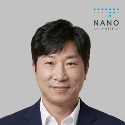
초청발표: AI-driven AFM for rapid exploration of material properties
Atomic force microscopy (AFM) has become a powerful tool for probing the physical properties of nanoscale materials and devices. However, conventional AFM measurements often require manual identification of regions of interest and expert-driven interpretation of large datasets, limiting measurement throughput and hindering efficient exploration of material properties. Recent advances in artificial intelligence (AI) offer new opportunities to automate AFM measurements and accelerate both data acquisition and analysis. In this presentation, I will introduce AI-driven AFM approaches for the rapid exploration of material properties. First, I will present an autonomous AFM workflow that employs machine learning-based image segmentation and clustering algorithms to automatically identify and characterize microstructural features in two-dimensional (2D) materials. By utilizing AFM's multimodal imaging capabilities, this approach enables simultaneous extraction of structural and electrical properties and their direct correlation across large datasets. I will also discuss AI-assisted strategies for autonomous measurement planning and high-throughput characterization. In addition, I will present deep learning approaches for enhancing the speed and sensitivity of piezoresponse force microscopy (PFM). By reconstructing high quality PFM images from sparsely sampled datasets, the proposed method substantially reduces measurement time while preserving quantitative information. In particular, I will demonstrate how domain images acquired within a few seconds can be reconstructed to a quality comparable to that obtained from conventional measurements requiring several minutes. These AI-assisted approaches minimize user intervention, improve measurement efficiency, and substantially increase throughput, providing a pathway toward autonomous, high-speed nanoscale characterization for accelerated materials research and discovery.
휴식(Coffee Break)
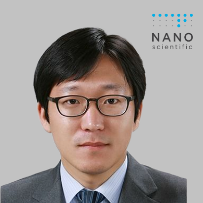
초청 발표: Switchable Plasmonic Nearfields in Conducting Polymer Nanoantennas Visualized by Photo-induced Force Microscopy
Conducting polymers are promising materials for active nanophotonics because their optical properties can be reversibly modulated through chemical or electrochemical doping. Highly doped conducting polymers can support infrared plasmonic resonances, enabling tunable nanoantenna-based light confinement. However, direct visualization of their local plasmonic near fields has remained challenging. Here, we use photoinduced force microscopy (PiFM) to directly visualize the near-field response of conducting polymer nanoantennas. Diameter-dependent PiFM measurements reveal localized near-field enhancement and a systematic spectral redshift with increasing nanodisk size. Comparison with far-field optical spectra and electromagnetic simulations shows a spectral offset between the far-field extinction and near-field intensity maxima, consistent with the strongly damped plasmonic response of conducting polymers. We further demonstrate redox-controlled switching of the near-field response by directly visualizing the suppression and recovery of plasmonic near fields. These results establish conducting polymer nanoantennas as a tunable platform for active infrared nanophotonics, molecular sensing, and reconfigurable light–matter interactions.
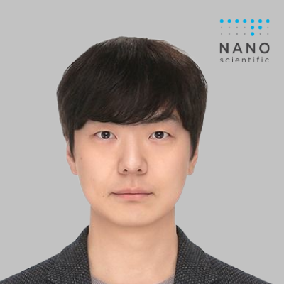
초청발표: 유무기 페로브스카이트 태양전지의 첨단 물성 연구와 반도체 소재 국소 화학조성 분석 - PiFM의 활용 연구
광유도력 현미경 (Photo-induced Force Microscopy, PiFM)은 원자힘현미경의 탐침과 시료표면 사이에 형성된 근접장을 이용하여, 광회절 한계를 넘어 나노스케일 영역의 적외선 분자진동 정보를 비파괴적으로 측정하는 분석기법이다. 본 발표에서는 파크시스템스의 FX200 IR 시스템을 이용하여 유무기 페로브스카이트 태양전지 및 반도체 소재 분석의 나노스케일 적외선 분광 연구 사례를 소개한다. 최근 본 연구진은 oleylamine 첨가와 vacuum-assisted 결정화로 성장시킨 유무기 페로브스카이트 흡수층에 대해, 단면 PiFM으로 유기 양이온의 특징적 진동 신호를 두께 방향으로 매핑함으로써 수직 정렬된 결정 성장을 화학적으로 규명하였다 [1]. 이 결과는 방사광 in situ GIWAXS 분석과 결합되어, 전구체 용액 내 결정 seed 형성부터 최종 박막의 결정 격자 정렬에 이르는 결정화 경로를 밝혔으며, 최종 박막의 뛰어난 태양전지 소자 특성을 설명하는 광흡수층의 나노스케일 국소 정렬을 뒷받침하는 핵심 근거가 되었다. 나아가 다양한 유무기 전자소자 소재를 대상으로 한 공동연구와 반도체 소재 표면의 국소 화학 성분 규명 사례를 통해, 나노스케일 화학 조성 분석 도구로서 PiFM이 갖는 범용적 활용 가치를 제시하고자 한다.
[1] S.-J. Kim, S. Hong, D.-G. Kwun, et al., Advanced Energy Materials 16 (2026) e06521

초청발표: Spectroscopic origin of photo-induced force
Photo-induced force microscopy (PiFM) enables nanoscale spectroscopic imaging by detecting optically induced forces between an illuminated probe and a sample. However, the physical origin and spectral interpretation of the measured force strongly depend on the optical and thermophysical properties of the material. In this talk, we distinguish two principal contributions: the photo-induced dipole force (PiDF), arising from optical field-gradient and scattering interactions, and the photo-induced thermal force (PiTF), generated by light absorption, thermal expansion, and the resulting modulation of the tip–sample interaction. Experimental examples involving plasmonic structures, polymers, crystalline quartz, amorphous silica, and native silicon oxide demonstrate that the relative contributions of PiDF and PiTF can be identified through their characteristic spectral line shapes and material-dependent oscillator strengths. Strong phonon resonances in crystalline SiO2 produce dipole-force-dominated spectra, whereas amorphous SiO2 primarily exhibits absorption-related thermal-force responses. These results establish a unified framework for interpreting PiFM spectra and clarify its complementary role alongside PTIR, AFM-IR, s-SNOM, and nano-FTIR for nanoscale chemical, optical, and structural characterization.
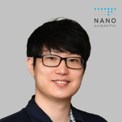
파크시스템스 발표: 2026 Research AFM Portfolio and Development Focus Areas

점심(Lunch Buffet)
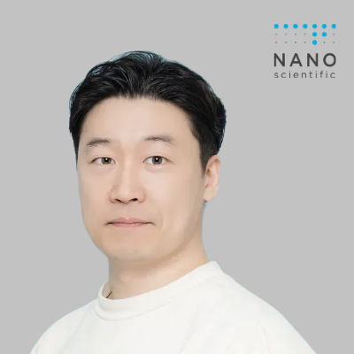
초청발표: Advanced PKG 제품의 주요 MI Challenge와 기술 개발 방향
The rapid expansion of AI and high-performance computing has accelerated the adoption of advanced packaging technologies, including HBM, 3D IC, Co-Packaged Optics (CPO), and panel-level packaging. As device architectures and manufacturing processes become increasingly diverse, metrology and inspection (MI) face new challenges that extend beyond conventional process control. Addressing these challenges requires not only product-specific solutions but also common technology foundations that can be leveraged across multiple advanced packaging platforms.
This presentation provides an overview of major advanced packaging technologies and discusses the corresponding MI requirements and technical challenges associated with HBM, 3D IC, CPO, and Panel applications. Key MI topics—including overlay, surface topography, warpage, and defect inspection—are examined to highlight both the unique requirements of each product and the common technical issues shared across different packaging platforms.
Finally, the presentation discusses common MI technology directions that can support multiple advanced packaging applications, emphasizing opportunities to transfer knowledge and technical capabilities across product domains. The evolving role of metrology and inspection in enabling robust manufacturing and future advanced packaging technologies will also be presented.
초청발표: 반도체 Surface Topography 계측 기술
반도체 산업이 공정 미세화를 넘어 3D 적층 구조로 진화함에 따라, MI(Metrology & Inspection) 기술은 단순한 치수 측정을 넘어 공정의 안정성과 수율을 좌우하는 핵심 인프라가 되었습니다. 특히 Surface Topography계측은 많은 부분 광학적 원리로 계측되고 있지만, 하부 구조의 복잡성과 물질 특성에 따른 회절 간섭 현상으로 인해 한계가 있습니다. 최근 Photo(EUV), CMP, Etch 및 Advanced Packaging 공정 고도화로 극한의 프로파일 및 평탄도 제어가 필요하며, 광학적 한계를 극복할 대안으로 물리적인 탐침으로 표면을 직접 스캔하는 원자 수준의 고해상 원자현미경(AFM) 기술이 필수 도구로 부각되고 있습니다.
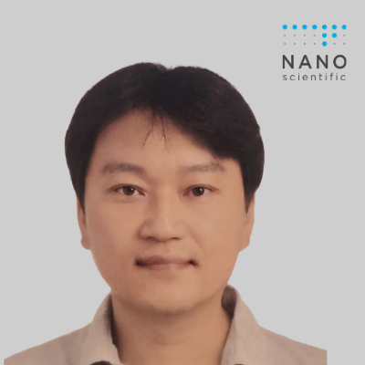
파크시스템스 발표: 2026 Industrial AFM Market Overview & Product Updates
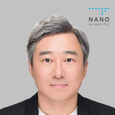
휴식
초청발표: Electrofludic Integration of Nano LEDs for Mobile and AR/VR Displays
Electofluidic assembly platform for nano-LEDs aimed at enabling next-generation high-resolution and large-area displays. Conventional micro-LED display manufacturing typically relies on the precise pick-and-place transfer of individual chips, which can result in long processing times, high equipment costs, and limited scalability for high-density or large-area applications. In contrast, the proposed approach disperses nano-LEDs in a liquid medium and selectively assembles them onto patterned substrates through controlled electrical and fluidic forces.
Our Electrofluidic assembly process enables the simultaneous placement of a large number of nano-LEDs, potentially improving throughput and simplifying fabrication compared with conventional serial transfer methods. By designing microscale receiving structures and electric-field conditions, the assembly location and orientation of nano-LEDs can be controlled to support dense pixel formation and improved optical uniformity.
The technology can be applied to a broad range of display platforms, including AR/VR microdisplays, automotive AR-HUDs, mobile and wearable displays, as well as transparent and flexible displays. With further development in large-area process stability, RGB color integration, electrical interconnection, and device reliability, fluidic nano-LED assembly is expected to provide a scalable manufacturing route for future inorganic emissive display technologies.
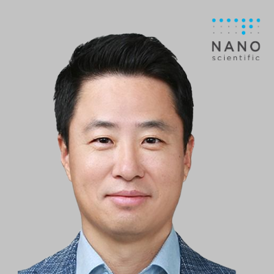
초청발표: Artificial Intelligence in Digital Holographic Imaging: Technical Basis and Biomedical Applications
Digital holographic imaging (DHI) has emerged as a powerful label-free imaging modality capable of quantitatively measuring the phase and amplitude information of transparent specimens. Recent advances in artificial intelligence (AI) have significantly expanded the capabilities of DHI by enabling high-quality image reconstruction, artifact suppression, super-resolution, virtual staining, and automated quantitative analysis. This presentation will first introduce the fundamental principles of digital holographic imaging and discuss the technical challenges associated with phase retrieval, noise reduction, and computational reconstruction. It will then present how modern AI techniques, including deep learning and physics-informed models, can overcome these limitations and improve both imaging performance and analysis accuracy. Finally, representative biomedical applications, such as label-free cell imaging, quantitative phase imaging, virtual fluorescence generation, and AI-assisted cellular analysis for disease diagnosis and drug discovery, will be highlighted. The integration of AI and digital holography is expected to play a key role in next-generation computational imaging and intelligent biomedical diagnostics.
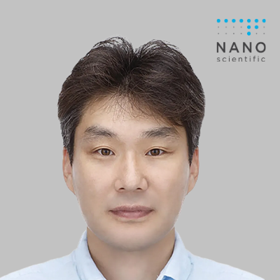
파크시스템스 발표: Seeing More with Park's Optical Metrology
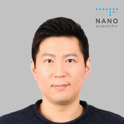
휴식
연구원 발표: AFM applications in 3D semiconductor integration
3D vertical stacking has emerged as an essential strategy to overcome the physical scaling limits of conventional semiconductor miniaturization and now underpins next generation devices such as high bandwidth memory (HBM). However, bonded interfaces inevitably suffer from thermal expansion mismatch, residual stress, delamination, and heat dissipation issues, and probing these buried interfaces at the nanoscale remains a formidable challenge. Here, we highlight how atomic force microscopy (AFM) serves as a comprehensive characterization platform across the entire 3D integration process, encompassing Cu hybrid bonding for heterogeneous integration and van der Waals monolithic integration under back-end-of-line compatible conditions. AFM topography directly evaluates the surface roughness and Cu pad dishing of chemical mechanical polishing processed wafers, which governs bonding yield. Force-distance spectroscopy quantifies interfacial adhesion and bonding energy, while nanomechanical mapping visualizes residual stress and warpage evolution at heterogeneous interfaces. In monolithic 3D integration, conductive AFM provides unprecedented insight into local crystallinity and conductive filament dynamics within grain boundaries, connecting interface quality to device functionality. These capabilities establish AFM as an indispensable bridge between interfacial behavior and wafer-scale manufacturing, while accelerating the commercialization of 3D integration technologies.

연구원 발표: Unveiling the origin of electrical switching through advanced AFM techniques
Emerging memory technologies have attracted significant attention as promising candidates for next-generation computing systems owing to their unique switching characteristics, low power consumption, and compatibility with neuromorphic computing architectures. Various switching mechanisms, including conductive filament formation, interface/contact modulation, and ferroelectric polarization, enable a wide range of memory functionalities. However, as device dimensions continue to scale down and material systems become increasingly complex, it is challenging to elucidate the origin of resistive switching using conventional electrical characterization alone. In this context, atomic force microscopy (AFM) has emerged as a powerful tool for directly visualizing local electrical properties and correlating them with structural and chemical information at the nanoscale owing to its high spatial resolution. In this presentation, we present our recent studies employing AFM-based characterization to investigate resistive switching in emerging memory devices. Specifically, we will discuss the spatial investigation of interfacial charge transfer in heterojunctions, the observation of ion migration under applied bias, and the quantitative evaluation of electrical uniformity in active layers. These studies demonstrate the value of nanoscale electrical mapping for understanding resistive switching mechanisms.
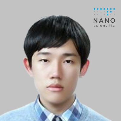
연구원 발표: Probing Nanoscale Light–Matter Interactions in Low-Dimensional Materials Using AFM-Based Near-Field Microscopy and Simulation
경품 추첨 및 폐회
만찬
Session 1 – 장비 시연 프로그램
Session 2 – 장비 시연 프로그램
점심식사 및 휴식
Session 3 – 장비 시연 프로그램
당일 차량 이용자는 파크시스템스 신사옥 지하 주차장에 주차하실 수 있으며, 가급적 지하 4층 또는 지하 5층에 주차해주시기 바랍니다.
1. 어반부티크 호텔(안양): 4호선 인덕원역 4번출구 도보 5분
2. AC 호텔 서울 금정 (군포): 1, 4호선 금정역 도보 6분
인근 서울 소재 호텔
3. 오라카이 청계산 호텔 (내곡동): 신분당선 청계산 입구역 1번 출구 도보 5분
4. 힐튼 가든 인 서울 강남 (서초동): 양재역 도보 3분
판교 소재 호텔
5. 나인트리 판교 (시흥동): 신분당선 판교역 1번출구 도보 5분
6. 더블트리 힐튼 판교(백현동): 수내역-정자역-판교역 순환 셔틀버스 운행
7. 코트야드 판교(삼평동): 신분당선 판교역 1번 출구 도보 12분
8. 그래비티 판교(백현동): 신분당선 판교역 1번 출구 도보 5분