Dr. Jack Alexander-Webber
Department of Materials, Loughborough University, UK
This article is based on his presentation delivered at the NanoScientific Forum Europe. Visit NanoScientific website to watch the full presentation: https://nanoscientific.org/on_demand
Introduction
The rapid emergence of advanced nanomaterials has created enormous opportunities for next-generation electronics, photonics, quantum devices, and sensing technologies. However, as material systems become increasingly sophisticated, one challenge continues to grow alongside them: characterization at scale.
Researchers today are no longer dealing with isolated nanoscale structures observed one at a time under a microscope. Modern nanoscience increasingly requires the ability to rapidly analyze large populations of nanoscale features while maintaining the precision necessary to understand subtle physical phenomena.
This challenge is particularly pronounced in emerging systems such as twisted bilayer graphene, transition metal dichalcogenide (TMD) heterostructures, and semiconductor nanowires, where small variations in geometry, orientation, or composition can dramatically alter electronic and optical behavior.
To address these challenges, researchers are increasingly combining imaging ellipsometry, optical microscopy, correlative imaging workflows, automated device integration, and machine learning into unified characterization pipelines capable of both nanoscale sensitivity and high-throughput analysis.
Twisted Bilayer Graphene and the Need for High-Throughput Characterization
Twisted bilayer graphene has become one of the most intensely studied material systems in modern condensed matter physics because its electronic and optical properties can change dramatically depending on the rotational angle between two graphene layers.
In conventional AB-stacked bilayer graphene, the material exhibits relatively well-understood behavior. However, introducing a rotational mismatch between the layers fundamentally modifies the electronic structure. Depending on the twist angle, researchers can observe enhanced optical absorption, altered band structures, and the emergence of strongly correlated electronic phenomena.
Practical graphene samples, however, are rarely perfectly uniform. Large-area chemical vapor deposition (CVD) growth often produces monolayer regions together with bilayer and multilayer inclusions, each potentially exhibiting different rotational domains and local optical responses.
Although conventional optical microscopy can reveal subtle color variations across these regions, the contrast is often weak and difficult to quantify reliably. This creates a major bottleneck for scalable characterization of twisted graphene systems
Imaging Ellipsometry as a High-Throughput Optical Probe
To overcome this limitation, the researchers employed spectroscopic imaging ellipsometry, a highly sensitive optical technique capable of mapping changes in polarization across a sample surface.
The experimental system combines a tunable wavelength light source, polarization control optics, an objective lens and camera-based imaging system to generate spatially resolved maps of optical behavior. Unlike traditional point-based optical measurements, imaging ellipsometry enables simultaneous analysis across extended sample areas.
This approach proved especially powerful for identifying subtle optical resonances associated with twisted bilayer graphene. The measurements revealed polarization-dependent resonance features that were nearly invisible in standard optical microscopy images.
These resonances originate from modifications in the electronic density of states caused by interactions between the twisted graphene layers. As the rotational angle changes, the optical absorption spectrum shifts accordingly.
By optimizing wavelength and polarization conditions, the researchers were able to maximize contrast between different graphene domains and rapidly map twist-angle variations across the sample surface 1. The wavelength-dependent optical response (Figure 1) also allowed resonance peaks to be correlated directly with graphene twist angles.
The result is a fast, non-destructive characterization method capable of probing large-area graphene samples while maintaining sensitivity to subtle electronic and optical variations.
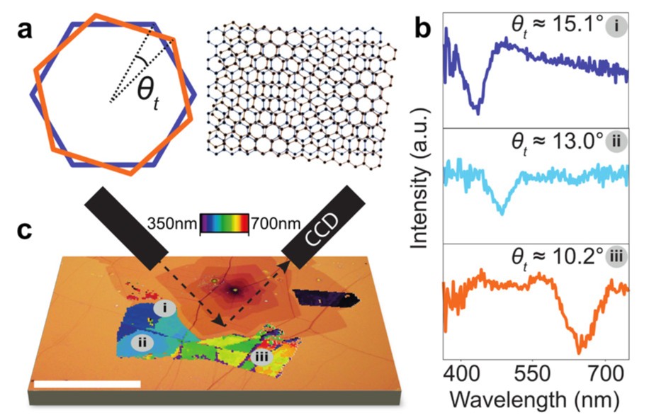
Figure 1. (A) Schematic of the first Brillouin zone (left) and crystal lattice (right) of twisted bilayer graphene with a twist angle of θt. (B) Example ellipsometric contrast microscopy spectra of twisted bilayer graphene with extracted θt labelled, taken from the regions identified in c. (C) Schematic incorporating an optical brightfield microscopy image of a CVD graphene multilayer region overlaid with resonant wavelength information (colourmap) obtained from spectroscopic ellipsometric contrast microscopy. Scale bar is 50 μm. Adapted from 1.
Large-Area Mapping of 2D Semiconductor Heterostructures
The same imaging ellipsometry techniques were extended to lateral 2D semiconductor heterostructures based on transition metal dichalcogenides.
These materials are synthesized by changing growth precursors during deposition, allowing one atomically thin material to nucleate laterally from another while remaining covalently bonded at the interface. Systems discussed included combinations such as molybdenum diselenide and tungsten diselenide, as well as sulfide-based heterostructures. Such heterostructures are particularly interesting because they can naturally form atomically thin PN junctions with useful optoelectronic behavior.
However, distinguishing adjacent material regions using conventional optical microscopy can be difficult because the intrinsic contrast is often extremely weak. The challenge becomes even greater when the materials are embedded within polymer layers or when substrate optical conditions change.
Imaging ellipsometry provides a significant advantage because both wavelength and polarization settings can be optimized specifically to enhance contrast between neighboring materials. Using these optimized conditions, researchers were able to rapidly identify material boundaries, segment different growth regions, and generate large-area statistical maps of heterostructure coverage and geometry 2.
Compared with slower point-based techniques such as Raman spectroscopy, the method offers a much faster approach for large-area materials analysis while still maintaining strong sensitivity to nanoscale optical inhomogeneities. These techniques can be extended to other lateral PN junctions such as those formed through selective oxidation of WSe2 3,4.
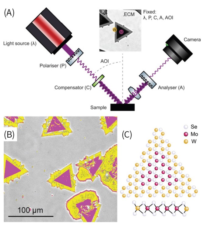
Figure 2. (A) Schematic of the Park Systems EP4 imaging ellipsometer setup. Inset shows a typical ECM image of lateral MoSe2–WSe2 heterostructures. (B) Image segmentation applied to an ECM image to identify WSe2 (pink), and MoSe2 (yellow) respectively. (C) Schematic atomic model of lateral MoSe2– WSe2 heterostructures. Adapted from 2.
Semiconductor Nanowires and Automated Device Integration
The presentation also explored semiconductor nanowires and the challenge of integrating them into scalable electronic devices.
Semiconductor nanowires are attractive for nanoscale electronics and optoelectronics because of their direct bandgap behavior, high carrier mobility, tunable geometries, and strong confinement effects. However, device fabrication workflows are often highly labor intensive.
Nanowires are typically grown vertically in dense forests before being transferred onto planar substrates for device fabrication. Researchers then traditionally identify individual nanowires manually using optical or electron microscopy before designing lithographic contacts around them 5.
To automate this process, the researchers developed a position-encoded fiducial marker system fabricated directly onto the substrate using electron beam lithography. These markers contain spatial information that can be recognized automatically during microscopy imaging 6.
After nanowire deposition, image analysis software identifies both the fiducial markers and the nanowire positions, generating a positional database that can then drive automated lithography pattern generation.
The workflow consists of several sequential stages:
- Nanowires are dispersed onto patterned substrates
- Optical or SEM images are acquired
- Fiducial markers and nanowires are automatically identified
- Positional databases are generated
- Lithographic electrode patterns are created automatically around selected nanowires
This approach transforms what was once a highly manual process into a scalable fabrication workflow capable of producing large numbers of nanowire devices with minimal operator intervention.
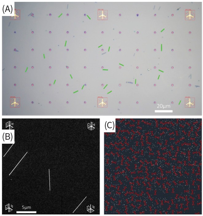
Figure 3. (A) Segmented optical brightfield reflection microscope image, (B) scanning electron microscope image of individualized InAs nanowires (coloured green in (A)) on an oxidized Si wafer patterned with machine readable “LithoTag” markers (labelled with red boxes in (A)) 6. (C) Position database of InAs nanowires (white) generated by high throughput microscopy and computer vision, overlaid with example automated device designs (red) aligned to selected individual nanowires.
Correlative Microscopy Across Multiple Imaging Platforms
An important aspect of the workflow is the integration of multiple microscopy modalities into a unified data system.
Using fiducial markers as common spatial references, the researchers correlated information from bright-field optical microscopy, dark-field optical microscopy, scanning electron microscopy, and lithographic device maps.
Because all datasets share the same positional framework, images acquired from different microscopes—even with different magnifications or optical configurations—can be aligned automatically.
This enables researchers to combine complementary information from multiple imaging systems while dramatically simplifying navigation and targeting across large sample areas.
The resulting datasets also provide statistically meaningful insight into device behavior. By fabricating and characterizing large numbers of nanowire devices, the researchers could observe systematic relationships between threshold voltage, nanowire diameter, channel length, and device geometry.
Toward Scalable and Data-Driven Nanotechnology Research
A common theme connecting all aspects of the work is the transition of nanoscience toward increasingly automated, scalable, and data-driven research workflows.
Historically, nanoscale characterization often depended on manual image interpretation, small experimental datasets, and labor-intensive fabrication processes. As nanotechnology moves closer to practical device integration and industrial-scale manufacturing, these approaches become increasingly difficult to scale.
By integrating imaging ellipsometry, correlative microscopy, automated lithography, computer vision, and machine learning into unified workflows, researchers are building research infrastructures capable of analyzing nanoscale systems with both statistical depth and nanoscale precision.
Importantly, these methodologies are broadly adaptable beyond the specific materials discussed here. Similar approaches could play important roles in wafer-scale 2D materials manufacturing, optoelectronic device screening, quantum materials research, and future AI-assisted nanomanufacturing environments.
Conclusion
High-throughput correlated microscopy is rapidly transforming nanoscience from a largely manual discipline into a scalable, data-driven research ecosystem. By combining advanced optical characterization, automated image analysis, correlative microscopy, and machine learning, researchers are increasingly able to study nanoscale materials with both statistical depth and nanoscale precision.
As emerging materials systems continue moving toward practical device integration and industrial-scale manufacturing, automated characterization and fabrication workflows are expected to become increasingly important. The integration of microscopy, data science, and intelligent automation is not only accelerating materials research, but also reshaping how future nanoelectronic technologies may ultimately be developed, optimized, and manufactured.
References
1. T. Potočnik et al. Fast Twist Angle Mapping of Bilayer Graphene Using Spectroscopic Ellipsometric Contrast Microscopy, Nano Letters, 23, 5506-5513 (2023). https://pubs.acs.org/doi/full/10.1021/acs.nanolett.3c00619
2. T. Potočnik et al. High-Throughput Ellipsometric Contrast Microscopy of Lateral 2D Heterostructures for Optoelectronics, Small Methods, 10, 2500437 (2026). https://onlinelibrary.wiley.com/doi/full/10.1002/smtd.202500437
3. J.-J. Lin et al. Ultra-Low Power CMOS Logic and Photodetection in WSe2 Semiconductors by Selective Area Plasma Doping, ACS Applied Materials & Interfaces, https://doi.org/10.1021/acsami.6c04479 (2026).
4. F. Abualnaja et al. Spectroscopic imaging ellipsometry for spatially resolved mapping of layer-by-layer oxidation in WSe2, Appl. Phys. Lett. 128, 211601 (2026). https://doi.org/10.1063/5.0320605
5. J.A. Alexander-Webber et al. Engineering the Photoresponse of InAs Nanowires, ACS Applied Materials and Interfaces, 9, 43993-44000 (2017). https://pubs.acs.org/doi/10.1021/acsami.7b14415
6. T. Potočnik et al. Automated Computer Vision-Enabled Manufacturing of Nanowire Devices, ACS Nano, 16, 18009-18017 (2022). https://pubs.acs.org/doi/10.1021/acsnano.2c08187

About Dr. Jack Alexander-Webber
Jack Alexander-Webber received his MSci in Physics from Royal Holloway, University of London (2009) and his DPhil in Condensed Matter Physics from the University of Oxford (2013). He joined the Electrical Engineering Division in the Department of Engineering, University of Cambridge in 2014 as a Junior Research Fellow of Churchill College. He subsequently held a Research Fellowship from the Royal Commission for the Exhibition of 1851. In 2019 Jack was awarded a Royal Society Dorothy Hodgkin Research Fellowship and now leads the Low-Dimensional Electronics Group. In 2026 Jack was appointed as a Senior Lecturer in Advanced Materials in the Department of Materials, Loughborough University.
The focus of his research is to develop a foundation of fundamental materials science and device engineering in novel electronic materials, and use the expertise and insights gained to demonstrate new (opto)electronic and quantum device concepts with enhanced performance and novel functionalities. His work has been published in leading journals including Nature, Science, Advanced Materials, ACS Nano, Nano Letters, Physical Review Letters, and Nature Communications, with >6000 citations to date. Jack co-authored the textbook, Quantum Technology (Elsevier, 2025), alongside Prof. Stefan Tappertzhofen to provide an accessible, engineering-focused introduction to the fundamentals and applications of quantum phenomena. Jack is also a co-founder of Nanomation Ltd., a startup developing scalable nanomaterial optoelectronic technologies.
NANOscientific Magazine, 2026