Puvaneswaran Chelvanathan, Solar Energy Research Institute (SERI) and Centre for Research Instrumentation and Management (CRIM), The National University of Malaysia, Malaysia
Presented at the NanoScientific Symposium India. This article incorporates findings from recent published research. Visit NanoScientific website to watch the full presentation: https://nanoscientific.org/on_demand
Understanding What Limits Next-Generation Thin-Film Solar Cells
As the world accelerates its transition toward renewable energy, solar photovoltaics (PV) continue to play a central role in reducing dependence on fossil fuels while reducing greenhouse gas emissions. Although crystalline silicon remains the dominant commercial technology, researchers continue to explore alternative photovoltaic materials that can reduce manufacturing costs, improve material utilization, and rely on earth-abundant elements. Among these emerging materials, copper zinc tin sulfide/selenide (CZTSSe) has attracted considerable interest because it combines excellent optical properties with environmentally benign and low-cost constituent elements.
Unlike conventional silicon solar cells, which require wafers more than one hundred micrometers thick, CZTSSe possesses a direct bandgap and a high optical absorption coefficient, allowing nearly all incident sunlight to be absorbed within an absorber layer approximately one micrometer thick. These characteristics make CZTSSe an attractive candidate for next-generation thin-film photovoltaics.
Despite these advantages, CZTSSe solar cells have not yet achieved the efficiencies of more mature technologies such as CdTe and CIGS. Improving their performance requires a deeper understanding of how nanoscale structural and electrical properties throughout the device influence macroscopic photovoltaic performance. To address this challenge, researchers at UKM have employed a suite of advanced atomic force microscopy (AFM) techniques to perform layer-by-layer nanoscale functional mapping of CZTSSe solar cells.
Why CZTSSe?
Thin-film photovoltaic technologies offer an attractive complement to conventional crystalline silicon because they can use much thinner absorber layers while enabling lightweight, flexible, and scalable device formats. Unlike crystalline silicon wafers, which are typically around 160 µm thick, thin-film solar cells can use absorber layers of only about 1–3 µm, reducing semiconductor material use by more than 95%. This makes thin films especially relevant for applications such as building-integrated photovoltaics, vehicle surfaces, agrivoltaics, and other form factors that are difficult to realize with brittle silicon wafers ¹.
Among established thin-film technologies, CdTe and CIGS have reached high levels of commercial maturity, with laboratory efficiencies above 23% and multi-gigawatt-scale production. However, each technology faces material-related concerns: CdTe involves cadmium and tellurium-related environmental or supply considerations, while CIGS depends on critical elements such as indium and gallium. Perovskites have achieved very high laboratory efficiencies, reaching 26.7% for single-junction cells, but long-term outdoor stability and lead management remain important challenges.
CZTSSe thin film solar cell (see Figure 1) is promising because it addresses some of these sustainability and scalability concerns. As a kesterite absorber based on copper, zinc, tin, sulfur, and selenium, it avoids indium and cadmium while relying largely on earth-abundant and comparatively non-toxic elements. The related CZTS material has a direct bandgap of about 1.4–1.6 eV and an absorption coefficient above 10⁴ cm⁻¹, allowing 1–2 µm films to harvest much of the terrestrial solar spectrum. Alloying sulfur with selenium to form CZTSSe further tunes the bandgap, extends minority-carrier diffusion lengths, and has enabled substantial efficiency improvements, including record CZTSSe efficiencies approaching 17%.
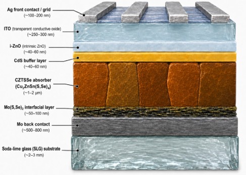
Figure 1. CZTSSe Thin Film Solar Cell Device
Despite this potential, CZTSSe still faces major scientific and engineering challenges. Its efficiency is limited by a large open-circuit-voltage deficit associated with Cu–Zn disorder, deep Sn-related defects, bandtail states, secondary phases, and recombination at grain boundaries and interfaces. The review also highlights that conventional CdS buffers can create unfavorable band alignment, while Mo back contacts may form resistive Mo(S,Se)₂ interfacial layers and promote Sn loss during selenization. These unresolved nanoscale and interfacial mechanisms make CZTSSe an important research platform for developing low-cost, earth-abundant thin-film photovoltaics with improved performance and long-term scalability.
Looking Beyond Conventional Characterization
Solar-cell performance is often evaluated through macroscopic measurements such as efficiency, open-circuit voltage, short-circuit current, and series resistance. While these measurements reveal how well a device performs, they do not explain why performance losses occur. Many of the critical processes governing charge transport happen at the nanoscale, particularly at interfaces between different layers of the solar-cell structure. Understanding these local variations requires characterization techniques capable of measuring not only surface morphology, but also electrical and photoelectrical behavior with nanometer-scale resolution.
Multimodal AFM provides this capability by combining topographical imaging with conductive and photo-conductive measurements. These techniques enable researchers to directly correlate local physical structure with functional electrical properties.
Revealing Hidden Conductivity Variations with Conductive AFM
The typical CZTSSe device consists of a glass substrate, a molybdenum (Mo) back contact, the CZTSSe absorber layer, a cadmium sulfide (CdS) buffer layer, transparent conductive oxides, and metallic front contacts. Although often viewed simply as an electrode, the molybdenum layer performs multiple functions simultaneously. It must provide excellent electrical conductivity while maintaining strong adhesion, chemical stability, moisture resistance, optical reflectance, and appropriate band alignment with the p-type absorber layer. Achieving all these requirements within a single deposited film is far from trivial.
To better understand the behavior of molybdenum back contacts, the research team investigated films deposited under different processing conditions and examined them using conductive AFM (C-AFM). Freshly deposited molybdenum films exposed to humid conditions rapidly developed native oxide layers. Conductive AFM identified localized regions of reduced conductivity associated with native molybdenum oxide formation. Conductive AFM measurements showed that these surface oxides reduced local conductivity by nearly an order of magnitude, corroborating with the Hall measurement data ².
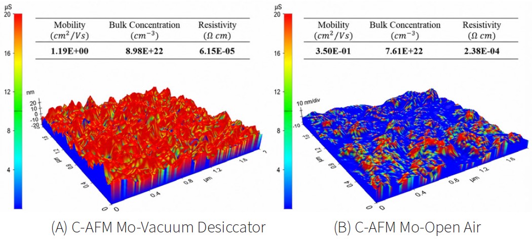
Figure 2. Surface conductance of Mo thin films kept in (A) vacuum desiccator and (B) open air.
This finding highlighted one of the key advantages of AFM-based electrical measurements: the ability to visualize local electrical heterogeneity at nanoscale resolution that may significantly affect device performance while remaining hidden in conventional bulk electrical measurements.
Engineering the Molybdenum Back Contact
An important challenge arises during sulfoselenization of the absorber layer, when sulfur diffuses into the molybdenum back contact and spontaneously forms an interfacial molybdenum disulfide (MoS₂) layer. Because this interfacial layer is not intentionally grown, its electrical properties can vary considerably, influencing band alignment and the formation of an effective ohmic contact. Simulation studies further indicated that the work function of the molybdenum back contact and the electrical characteristics of the MoS₂ interfacial layer play critical roles in determining carrier transport across the interface ³. These observations motivated a detailed nanoscale investigation using multimodal AFM.
Subsequent optimization focused on improving the molybdenum layer itself was carried out focusing on how post-deposition vacuum annealing modifies molybdenum (Mo) back contacts for CZTSSe thin-film solar cells ⁴. The vacuum-annealed Mo showed a stronger preferred crystallographic orientation, larger and more compact grains, lower surface roughness, and a much lower resistivity of 16.89 μΩ.cm compared with 61.53 μΩ.cm for the as-sputtered Mo. It also exhibited a higher work function of about 5.05 eV, compared with approximately 4.78 eV for the untreated Mo.
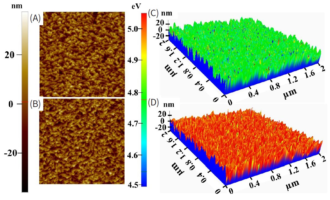
Figure 3. AFM topography image of (A) As-Sputtered Mo, (B) Vacuum Annealed Mo and work function overlay on z-height of (C) As-Sputtered Mo, (D) Vacuum Annealed Mo
These improvements also enhanced the Mo/CZTSSe interface. During selenization, the as-sputtered Mo promoted thicker and less favorable MoSe₂/Mo(S,Se)₂ interfacial formation, including mixed orientations that hindered adhesion and charge transport. In contrast, the vacuum-annealed Mo reduced interfacial layer formation and favored a more beneficial vertically aligned MoSe₂ orientation, providing a lower-resistance pathway for carrier transport. The annealing treatment also enabled sodium diffusion from the soda-lime glass substrate through the Mo layer, which enhanced the crystallinity and grain growth of the CZTSSe absorber. As a result, devices fabricated on vacuum-annealed Mo achieved a power conversion efficiency of 7.70%, far higher than the 0.71% efficiency obtained using as-sputtered Mo.
Visualizing Nanoscale Defects in the Absorber Layer
The investigation extended beyond the back contact into the CZTSSe absorber itself. Certain regions of the absorber surface exhibited unusual optical reflectivity and were selected for detailed AFM examination. Conductive AFM revealed localized defects, including pinholes and debris structures, that displayed unexpected electrical behavior. Interestingly, some pinholes that were expected to expose highly conductive molybdenum underneath showed little or no conductivity enhancement.
To understand this phenomenon, the researchers performed correlative field emission scanning electron microscopy (FESEM) analysis. The results revealed the presence of secondary phases, including tin sulfide compounds, occupying these regions. Rather than exposing the conductive molybdenum back contact as initially expected, these secondary phases altered the local electrical pathways and explained the unusual conductivity observed by conductive AFM.
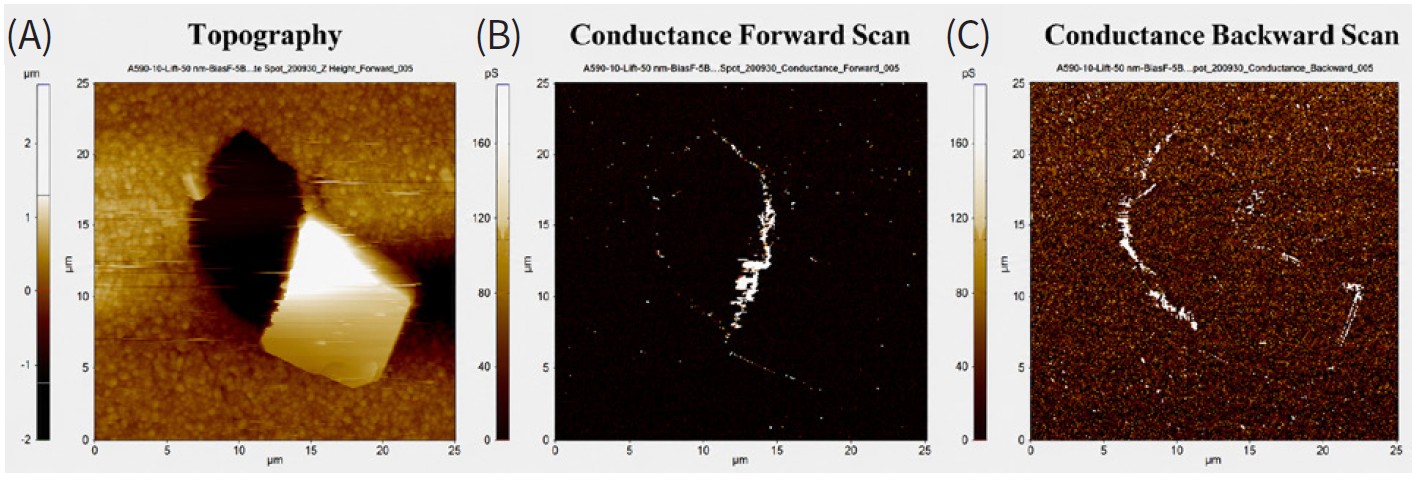
Figure 4. (A) Topography of micro-pinhole and secondary phase segregation with its nanoscale conductance variation in (B) forward scan and (C) backward scan
These observations demonstrated how local compositional variations can dramatically alter electrical transport pathways within the device, providing important clues regarding performance-limiting mechanisms.
Probing Photoresponse at the Nanoscale
The cadmium sulfide buffer layer represents another critical component of CZTSSe solar cells. Using photoconductive AFM, the research team illuminated CdS films with laser excitation while monitoring the local electrical response. Because CdS has a band gap of approximately 2.4 eV, illumination with a 405 nm laser corresponds to a photon energy of about 3.06 eV, which is above the CdS band gap. Therefore, the observed increase in conductivity under 405 nm illumination is consistent with direct photon absorption and photocarrier generation in the CdS layer.
However, measurements using longer-wavelength illumination, with photon energies closer to or below the CdS band gap, could provide additional insight into sub-bandgap photoresponse mechanisms. Such experiments may help identify band-tail states, defect-related states, or localized electronic states within the CdS thin film that could contribute to additional optical absorption pathways. These possibilities highlight the potential of photoconductive AFM for probing nanoscale photoelectrical behavior and electronic structure in semiconducting buffer layer.
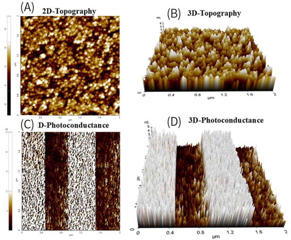
Figure 5. (A) and (C) 2D topography and photoconductance of CdS thin film and its corresponding (B) and (D) 3D topography and photoconductance
Such nanoscale photoelectrical measurements provide valuable insight into the electronic properties of thin-film photovoltaic materials that are difficult to obtain using conventional optical characterization techniques alone.
Conclusion: Toward Higher-Efficiency Earth-Abundant Solar Cells
Although CZTSSe technology still trails the efficiency records achieved by silicon, CIGS, and perovskite solar cells, its combination of earth-abundant elements, low toxicity, and long-term stability continues to make it an attractive candidate for future photovoltaic applications.
As photovoltaic research increasingly focuses on understanding complex material systems at ever smaller scales, nanoscale functional mapping will continue to play a vital role in bridging the gap between material properties and device performance.
The studies presented here demonstrate how advanced AFM techniques can reveal critical nanoscale processes that influence device behavior. By combining conductive AFM, photo-conductive AFM, and correlative microscopy, researchers can directly relate nanoscale functional properties to macroscopic photovoltaic parameters such as open-circuit voltage, short-circuit current, and series resistance. This multimodal approach provides valuable insight into the structural and electrical origins of device performance, guiding the continued development of more efficient thin-film solar cells.
About Dr. Puvaneswaran Chelvanathan
Dr. Puvaneswaran Chelvanathan is a Senior Lecturer and Research Fellow at the Solar Energy Research Institute (SERI) and the Centre for Research Instrumentation and Management (CRIM) at Universiti Kebangsaan Malaysia (UKM). Supported by the Malaysian Public Service scholarship during his early academic path, he completed his entire higher education at UKM, earning a B.Eng. in Microelectronics (2009), an M.Sc. in Electrical, Electronic, and Systems Engineering (2012), and a Ph.D. in Renewable Energy (2016). He embarked on research into thin-film solar cell science and technology in 2008, laying a solid foundation during his doctoral research which focused specifically on developing CZTS solar cells via magnetron sputtering. Following a nearly three-year tenure as a post-doctoral research fellow at SERI, he officially joined SERI as a research fellow to lead the thin film photovoltaic research group.
Today, Dr. Chelvanathan’s primary research centers on developing earth-abundant, low-cost, and highly scalable thin-film solar photovoltaic technologies capable of supporting true terawatt-scale energy deployment. As an expert in semiconductor optoelectronics, his technical pursuits bridge macroscopic device architectures with nanoscale functional mapping, making extensive use of multi-modal atomic force microscopy (AFM) and numerical simulations to eliminate performance-limiting defects. His prolific contributions to the field include extensive publication and ongoing investigation into emerging PV materials, such as perovskites, CZTSSe, and CIGS heterostructures, positioning his laboratory as a vital contributor to next-generation green energy solutions.
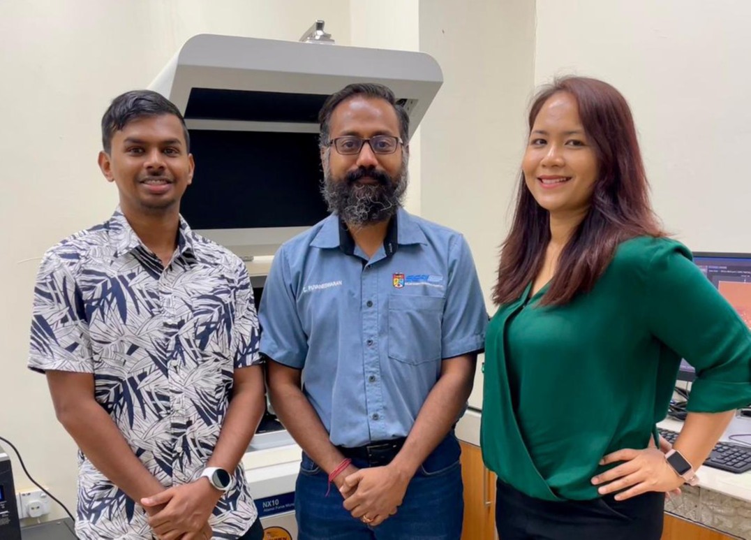
From left to right: Yoganash, Dr. Puvaneswaran Chelvanathan, Puteri.
References
- D. Intal, A. U. Ebong. Thin-film solar photovoltaics: Trends and future directions. Renewable and Sustainable Energy Reviews 226 (2026) 116464. DOI: 10.1016/j.rser.2025.116464.
- Y. Putthisigamany, K. S. Rahman, M. M. I. Sapeli, S. Shafian, U. Syafiq, M. S. Su’ait, N. A. Ludin, M. A. Ibrahim, P. Chelvanathan. Native surface oxidation phenomena of DC-Sputtered molybdenum thin film in tropical environment. Materials Letters 370 (2024) 136787. DOI: 10.1016/j.matlet.2024.136787.
- Y. Putthisigamany, K. S. Rahman, M. M. I. Sapeli, N. A. Ludin, M. A. Ibrahim, P. Chelvanathan. Revealing the subtle role of DC-sputtered Mo back contact work function in mitigating the detrimental effects of the MoS₂/MoSe₂ interfacial layer in kesterite-based thin film solar cells. Energy & Fuels (2024). DOI: 10.1021/acs.energyfuels.4c00512.
- Y. Putthisigamany, M. I. Hossain, A. Zekri, B. Aïssa, K. S. Rahman, M. M. I. Sapeli, M. S. Su’ait, N. A. Ludin, M. A. Ibrahim, P. Chelvanathan. Manifold benefits of vacuum annealed molybdenum back contact for enhanced CZTSSe thin film properties and device. Solar Energy Materials and Solar Cells 292 (2025) 113782. DOI: 10.1016/j.solmat.2025.113782.
NANOscientific Magazine, 2026