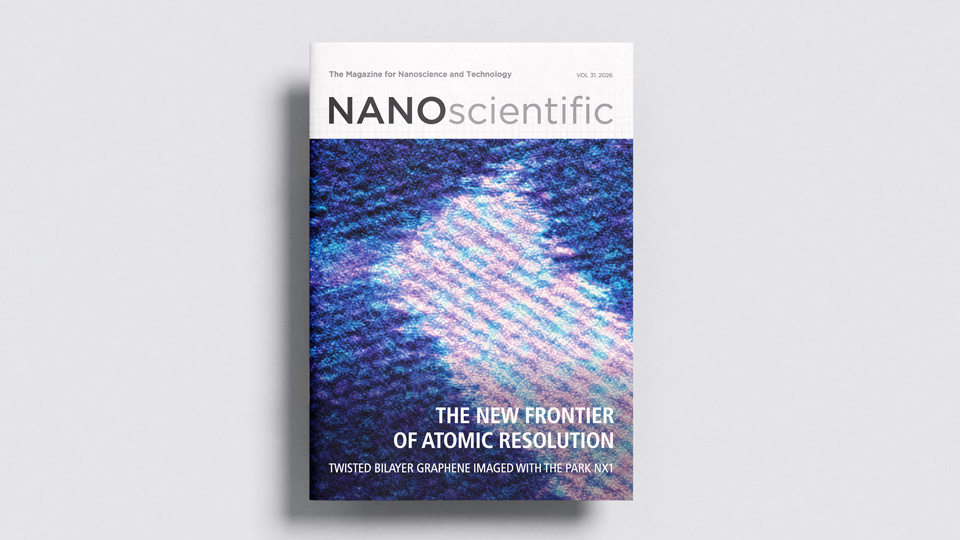
Park Systems Launches NX1: Bringing Atomic Resolution to Everyday Laboratory Environments
Park Systems has introduced the NX1, a new atomic force microscope (AFM) designed to deliver atomic-resolution imaging under ambient laboratory conditions. Developed in collaboration with Prof. Franz J. Giessibl of the University of Regensburg, the system transforms a research prototype into a commercial instrument, enabling a level of performance that has traditionally required ultra-high vacuum environments.
The NX1 is based on the Orpheus II research platform developed by Prof. Giessibl's group, which demonstrated that true atomic-resolution imaging could be achieved in air. Park Systems refined this concept into a fully engineered commercial instrument, combining the original thermally stable Kovar-based mechanical architecture with the company's expertise in precision manufacturing, automation, and long-term instrument reliability.
One of the NX1's defining characteristics is its exceptionally low mechanical noise floor, supported by a rigid, compact structure and a minimized mechanical loop. These design features help reduce vibration, thermal drift, and environmental disturbances that typically limit atomic-scale imaging under ambient conditions. The result is stable, repeatable measurements capable of resolving atomic lattices without the need for specialized vacuum systems.
Beyond imaging performance, the NX1 emphasizes ease of operation. Automated laser alignment, simplified probe exchange, an on-axis optical microscope, and compatibility with multiple AFM operating modes make the system accessible to a broader range of researchers while maintaining the precision required for advanced nanoscience investigations. Optional support for qPlus sensors further expands its capabilities for specialized applications.
The launch represents an important milestone for atomic force microscopy. By making atomic-resolution imaging practical in standard laboratory environments, the NX1 lowers the barriers to studying surfaces and interfaces at the atomic scale. Researchers working in quantum materials, semiconductors, catalysis, nanomaterials, and surface science can now perform routine atomic-scale characterization with greater convenience and accessibility, opening new opportunities for both fundamental research and advanced materials development.

(Left to right) Prof. Franz J. Giessibl (University of Regensburg) and Dr. Sang-il Park (Founder & CEO, Park Systems)
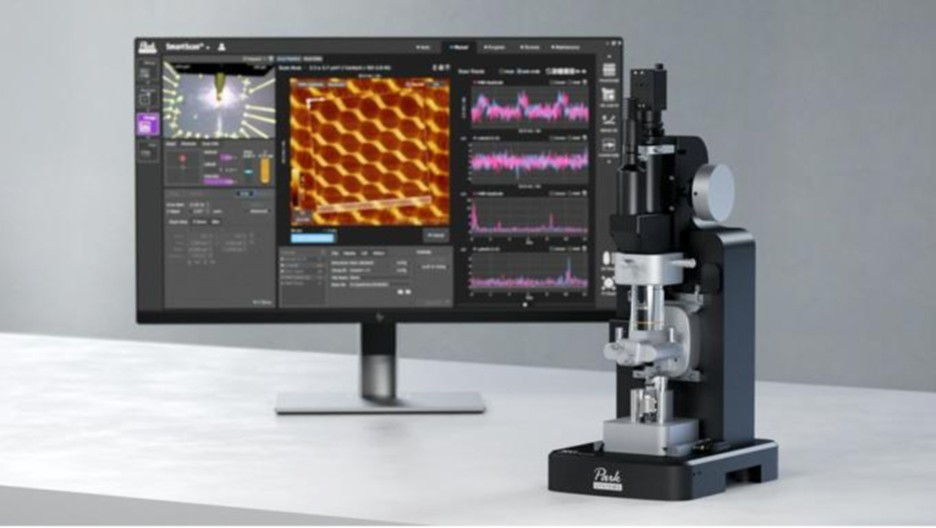
The Park NX1 Atomic Force Microscope, designed for atomic-scale imaging in ambient conditions.
Park Systems and imec Launch Joint Development Program for Next-Generation Semiconductor Metrology
Park Systems has announced a new Joint Development Program (JDP) with imec, one of the world's leading semiconductor research and innovation centers, to develop advanced metrology solutions for next-generation semiconductor manufacturing. The collaboration will focus on the increasingly demanding measurement challenges associated with advanced 3D packaging, heterogeneous integration, and future logic technologies.
As semiconductor devices continue to evolve beyond traditional transistor scaling, advanced packaging technologies—including chiplets, hybrid bonding, and complex three-dimensional architectures—require measurement techniques capable of accurately characterizing features at the nanometer scale. Through the partnership, imec will provide research samples based on its advanced packaging and logic technology roadmaps, enabling Park Systems to evaluate and further develop measurement solutions under realistic process conditions.
Unlike collaborations centered on a single instrument, the program will leverage Park Systems' expanding metrology portfolio. In addition to its industry-leading atomic force microscopy (AFM) systems, the company will evaluate complementary technologies including White Light Interferometry (WLI), Imaging Spectroscopic Ellipsometry (ISE), and Digital Holographic Microscopy (DHM). Together, these techniques provide a more comprehensive characterization workflow for increasingly complex semiconductor structures.
The two-year agreement also includes Park Systems' participation in imec's Industrial Affiliation Program (IIAP) for 3D System Integration, strengthening collaboration with researchers working at the forefront of semiconductor technology development. The partnership reflects the industry's growing recognition that future manufacturing advances will depend not only on new device architectures but also on equally sophisticated measurement capabilities.
For Park Systems, the JDP represents another step in expanding beyond traditional AFM into a broader nanometrology platform. By combining multiple complementary measurement technologies with imec's world-class semiconductor research infrastructure, the collaboration aims to accelerate the development of metrology solutions that can support the next generation of high-performance computing, artificial intelligence, memory, and advanced packaging technologies.
NANOscientific Magazine, 2026