Nearly every digital camera, from smartphones to scientific imaging systems, relies on a technology that has changed surprisingly little over the past two decades. While image sensors have become smaller, faster, and more sensitive, they still depend on tiny color filters placed over individual pixels to distinguish red, green, and blue light. These filters make color photography possible, but they also create one of the greatest inefficiencies in modern imaging by blocking much of the light before it ever reaches the sensor.
Researchers at ETH Zürich and Empa have now demonstrated an entirely different approach that could fundamentally change how cameras capture color. Instead of using passive filters that discard unwanted wavelengths, they developed a vertically stacked photodetector in which each layer naturally absorbs a different portion of the visible spectrum. Built from thin films of lead-halide perovskites, the prototype simultaneously improves light utilization, color fidelity, and spatial resolution while eliminating many of the limitations that have accompanied conventional color sensors for decades.
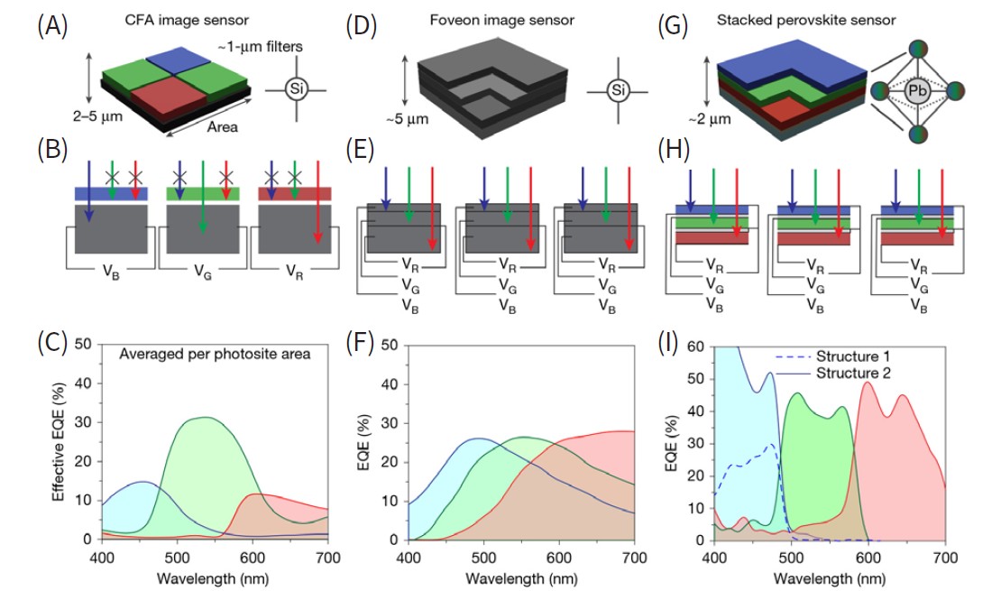
Figure 1. Schematics, architecture and EQE spectra of different image sensor architectures. (A)-(C) Bayer CFA sensor, in which color filters reduce the light reaching individual red, green, and blue pixels and lower overall EQE. (D)–(F), Foveon sensor, which uses vertically stacked silicon photodetectors to improve light utilization but provides limited color selectivity. (G)–(I), Monolithically stacked perovskite sensor, in which color-selective perovskite layers act as active optical filters, achieving higher quantum efficiency and improved color accuracy.
Why Today's Cameras Waste So Much Light
Conventional digital cameras use what is known as a Bayer color filter array (CFA). Each pixel is covered by either a red, green, or blue filter, allowing only that color to reach the underlying silicon detector while absorbing the remaining wavelengths. Every group of four pixels contains two green pixels, one red pixel, and one blue pixel, roughly mimicking the sensitivity of the human eye.
Although this architecture has proven remarkably successful, it comes with unavoidable compromises. Since each filter blocks approximately two-thirds of the incoming light, only a fraction of the available photons actually contribute to the image. The remaining light is simply lost as heat. In addition, because every pixel measures only one color, sophisticated image-processing algorithms must estimate the missing color information from neighboring pixels through a process known as demosaicing. While modern software performs this task impressively well, interpolation inevitably reduces image sharpness and can introduce artifacts such as false colors and moiré patterns, particularly in scenes containing fine textures.
These limitations become increasingly important in applications where every photon matters, including low-light photography, fluorescence microscopy, astronomy, biomedical imaging, and machine vision.
Learning from Earlier Stacked Sensors
The idea of stacking photodetectors is not entirely new. Sigma's Foveon image sensor attempted to solve many of the shortcomings of Bayer filters by placing three silicon photodiodes vertically within each pixel. Because blue light is absorbed near the surface of silicon while longer wavelengths penetrate deeper, the three layers collect different portions of the visible spectrum without requiring external color filters.
In theory, this allows every pixel to capture full-color information.
In practice, however, silicon is not naturally color selective. Its absorption changes gradually with wavelength, causing substantial overlap between the red, green, and blue channels. This overlap complicates color reconstruction and requires significant computational correction to produce realistic images. Although Foveon sensors eliminate many of the interpolation artifacts associated with Bayer filters, they have never achieved widespread adoption because of these challenges.
Why Perovskites Offer a Better Solution
Lead-halide perovskites have emerged as one of the most exciting classes of semiconductor materials over the past decade. Much of their appeal comes from the fact that their optical properties can be precisely tailored simply by adjusting their chemical composition. By changing the ratio of iodine, bromine, and chlorine within the crystal structure, researchers can tune exactly which wavelengths each material absorbs.
This capability makes perovskites ideally suited for vertically stacked color detectors. Rather than depending on the gradual absorption profile of silicon, each perovskite layer can be engineered to respond primarily to one region of the visible spectrum.
In the new device, the uppermost layer absorbs predominantly blue light, the middle layer detects green wavelengths, and the bottom layer captures red light. Because each layer acts as both an optical filter and a photodetector, incoming photons are converted directly into electrical signals instead of being discarded by passive filters. The result is a far more efficient use of the available light.
Building Three Photodetectors into One Pixel
Transforming this elegant concept into a working device required overcoming several significant fabrication challenges. Depositing one perovskite layer using conventional solution-processing techniques typically dissolves the layer beneath it, making multilayer structures extremely difficult to manufacture.
The research team solved this problem by depositing all perovskite absorber layers using vacuum co-evaporation. This technique produced smooth, pinhole-free films while preserving the integrity of the underlying layers. Each color-sensitive layer was combined with transparent electrodes, charge-transport materials, and dielectric spacers to form three independent photodiodes stacked vertically within a single photosite.
Cross-sectional electron microscopy clearly revealed the highly ordered multilayer architecture, with each functional layer carefully integrated into a structure only a few micrometers thick.
Capturing Nearly Twice as Much Useful Light
One of the most impressive achievements of the new sensor is its ability to utilize incoming light much more efficiently than conventional color cameras.
The researchers measured external quantum efficiencies of approximately 50% for the red channel, 47% for the green channel, and 53% for the blue channel. When averaged across an entire photosite, the stacked architecture achieved nearly twice the effective light utilization of a conventional Bayer color-filter array because very little of the incoming light is intentionally discarded.
In practical terms, this means more photons contribute directly to image formation. Improved photon efficiency can translate into brighter images, reduced exposure times, lower image noise, and improved performance under dim illumination—all highly desirable characteristics for scientific instruments as well as consumer cameras.
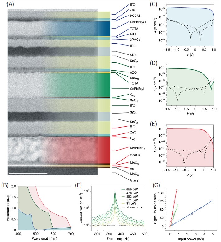
Figure 2. Stacked-detector architecture Cross-sectional electron microscopy image of the vertically stacked perovskite photodetector. Three independently optimized photodiodes are integrated within a multilayer structure only a few micrometers thick.
Reproducing Colors More Faithfully
Capturing more light is only valuable if colors remain accurate. To evaluate this aspect of performance, the researchers used a standard Macbeth ColorChecker, a calibration target widely employed throughout photography and imaging science.
Each colored patch reflects a carefully characterized spectrum of light. By illuminating the chart and recording the responses from each of the stacked detector layers, the researchers reconstructed the colors and compared them with internationally accepted color standards.
After calibration, the sensor achieved a color difference of ΔE = 3.8 in the CIELAB color space, outperforming both conventional Bayer sensors and Foveon-type architectures. More importantly, only modest computational correction was required because the perovskite layers already possess strong intrinsic wavelength selectivity. Unlike silicon-based stacked sensors, where significant overlap exists between color channels, the perovskite device naturally separates red, green, and blue light before any software processing begins.
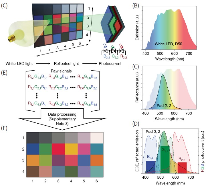
Figure 3. Stacked-detector color accuracy. (A) Color-accuracy measurement setup. (B) Emission spectrum of the white LED illuminating the ColorChecker. (C) Reflectance spectrum of a green ColorChecker patch [2, 2]. (D) RGB photocurrent responses from the stacked detector to the reflected light. (E) Matrix of measured RGB photocurrents for the ColorChecker patches. (F) ColorChecker image reconstructed from the three color channels of the stacked-perovskite detector.
Eliminating the Need for Demosaicing
Perhaps the greatest conceptual advantage of the vertically stacked design is that every pixel independently records complete color information. Since no interpolation is required, the entire demosaicing process disappears.
To demonstrate this benefit, the researchers fabricated prototype detector arrays and compared their imaging performance with simulated Bayer sensors. Images reconstructed using Bayer sampling showed the expected interpolation artifacts and reduced spatial resolution, whereas the stacked detectors produced cleaner images with improved preservation of fine detail.
Although the current prototypes contain relatively small arrays, the experiments clearly demonstrate the fundamental advantage of recording all three color channels at every pixel location.
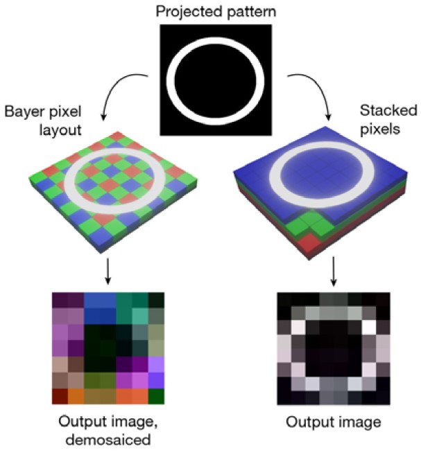
Figure 4. Imaging with monolithically stacked-detector arrays in cross-bar configuration. Comparison of reconstructed images. Conventional Bayer sensors require demosaicing, introducing color artifacts, whereas the stacked detector captures complete color information at every pixel, eliminating these artifacts.
Smaller Cameras with Better Performance
The advantages of perovskites extend beyond image quality alone.
These materials possess exceptionally high optical absorption coefficients, allowing visible light to be absorbed within films only a few hundred nanometers thick. Traditional silicon sensors generally require much thicker absorbing regions to collect the same amount of light.
Such compact detector structures could eventually enable thinner image sensors, shorter optical paths, and simpler lens designs. Smartphone cameras, wearable devices, endoscopes, and compact scientific instruments could all benefit from reduced size while maintaining—or even improving—image quality.
The vertical architecture also provides additional design flexibility. Because the spacing between detector layers can be engineered, future devices may even compensate for chromatic aberration within the optical system itself, reducing another long-standing source of image degradation.
Beyond Consumer Photography
Although consumer cameras provide the most familiar example, the potential applications of vertically stacked perovskite detectors extend much further.
Modern scientific imaging increasingly depends on extracting the maximum amount of information from extremely limited numbers of photons. Fluorescence microscopy, biomedical diagnostics, astronomy, industrial inspection, robotics, and autonomous vehicles all require sensors capable of distinguishing subtle spectral differences while maintaining high sensitivity.
Perovskites offer an additional advantage because their absorption characteristics can be precisely engineered over a broad wavelength range. Future generations of these detectors could therefore move beyond conventional RGB imaging toward multispectral or hyperspectral cameras capable of distinguishing colors and spectral signatures that are invisible to today's sensors.
Ensuring Quality at the Nanoscale
Surface morphology is an important consideration in the fabrication of vertically stacked optoelectronic devices, where nanoscale roughness and defects can affect interfaces between successive layers. As part of the material characterization, the researchers used a Park Systems NX10 AFM operating in non-contact mode with AC160TS cantilevers to examine the surface morphology of the perovskite films. AFM measurements were performed over 2 × 2 μm scan areas, complementing the optical, electrical, and electron microscopy techniques used to characterize the materials and completed devices.
Looking Ahead
Despite its impressive performance, the technology remains at the research prototype stage. Commercial implementation will require significant advances in multilayer lithography, high-density pixel fabrication, vertical electrical interconnects, long-term environmental stability, and integration with conventional CMOS image sensor electronics. Nevertheless, none of these challenges appears fundamentally prohibitive, and the rapid pace of progress in perovskite optoelectronics suggests that many could be overcome in the coming years.
For decades, digital cameras have accepted the loss of most incoming light as an unavoidable consequence of color imaging. This work challenges that assumption by demonstrating that vertically stacked, color-selective perovskite photodetectors can simultaneously improve photon efficiency, color accuracy, and spatial resolution while eliminating the need for conventional color filters and demosaicing algorithms. The prototype achieved external quantum efficiencies approaching 50% across all three color channels and demonstrated a calibrated color accuracy superior to today's mainstream sensor technologies.
As materials engineering, device fabrication, and sensor integration continue to mature, vertically stacked perovskite photodetectors could represent one of the most significant advances in digital imaging since the introduction of the Bayer color filter itself. From smartphones and scientific instruments to autonomous systems and machine vision, the next generation of cameras may ultimately capture more light, reproduce colors more faithfully, and reveal details that today's image sensors simply cannot see.
NANOscientific Magazine, 2026