Mohammad Alshoul, Xinchen Wang, Zimo Wang, and Jia Deng
Binghamton University, NY, USA
Based on "Investigation of Experimental Parameters in the Electric Field and Mechanical Vibration Integrated AFM-Based Nanopatterning on PEDOT," Manufacturing Letters, Vol. 41, 2024, pp. 546–557. Adapted under the Creative Commons Attribution 4.0 License.
Atomic force microscopy is best known as a powerful tool for imaging and characterizing surfaces at the nanoscale. However, the ability of an AFM probe to interact directly with a material also makes the technique attractive for nanomanufacturing. By controlling the motion, force, and electrical properties of the probe, AFM systems can be used to create nanoscale structures without the masks and complex processing infrastructure required by many conventional lithography techniques.
Researchers at Binghamton University have investigated an approach that combines an electric field with controlled mechanical vibration to improve AFM-based nanopatterning. Their study focuses on PEDOT:PSS, a conductive polymer widely investigated for applications in organic electronics, sensors, electromagnetic shielding, and optoelectronic devices. Using a systematic design-of-experiments approach, the researchers examined how applied voltage, patterning speed, and vibration trajectory affect the dimensions of nanoscale trenches produced in PEDOT:PSS films.
The results demonstrate that these parameters can be used as complementary controls over feature width and depth. In particular, the trajectory of the mechanical vibration strongly influences both the dimensions of the resulting structures and the range of conditions under which successful nanopatterning can occur.
AFM as a Nanomanufacturing Platform
High-resolution nanofabrication is essential for technologies including microelectromechanical and nanoelectromechanical systems, photonics, sensors, and emerging organic electronic devices. While established lithography methods can create extremely small structures, AFM-based approaches offer several advantages for research and specialized manufacturing. They are maskless, directly programmable, and capable of modifying selected areas of a surface with nanoscale precision.
Mechanical nanomachining can be performed by using an AFM probe as a nanoscale cutting or scratching tool. Introducing vibration into this process can further improve machining performance. Previous research has shown that vibration-assisted nanomachining can reduce machining forces and probe wear while enabling more complex two- and three-dimensional structures.
Electric fields provide another mechanism for controlling nanoscale material modification. When an electrical bias is applied between a conductive AFM probe and a sample, highly localized interactions can occur near the probe apex. Combining this electrical effect with mechanical vibration creates a hybrid nanopatterning process in which multiple parameters can be adjusted to control the resulting structures.
The Binghamton University researchers sought to better understand these interactions by quantitatively examining how electrical voltage and patterning speed behave under different vibration trajectories.
Creating Controlled Vibration Trajectories
The experiments were conducted using a Park Systems XE7 AFM equipped with a low-stiffness conductive contact probe having a nominal tip radius of 35 nm and a spring constant of 0.11 N/m. The probe was connected to a voltage source to establish the electrical potential required for electric-field-assisted lithography.
The researchers also developed a custom nanolithography stage incorporating two piezoelectric actuators oriented along the X and Y axes. By controlling the signals supplied to these actuators, the sample could be subjected to different vibration trajectories during patterning.
Two configurations were investigated. In the first, both X- and Y-axis actuators were driven with sinusoidal signals separated by a 90° phase difference, producing a circular vibration trajectory. In the second configuration, only the Y-axis actuator was used, generating a reciprocating motion.
The vibration frequency was maintained at 2 kHz with an amplitude of 0.2 Vpp, while the normal force was fixed at 2 nN. The researchers then varied two primary processing parameters: the applied voltage and the patterning speed.
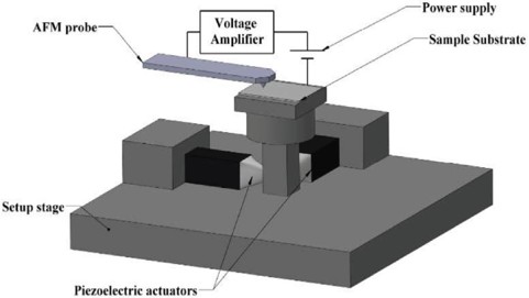
Figure 1. Schematic diagram of the experimental setup for electrical field and vibration-assisted AFM-based nanopatterning.
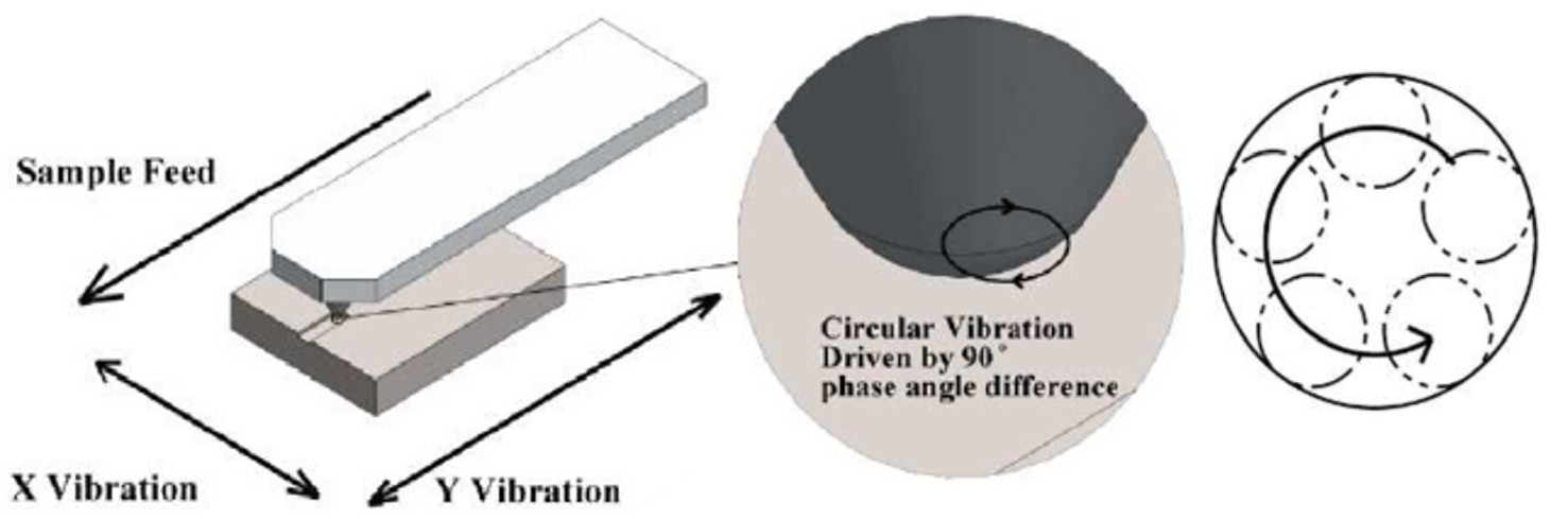
Figure 2. The circular trajectory introduced by XY-vibration.
The test material consisted of a 65-nm-thick PEDOT:PSS film spin-coated onto a highly doped silicon substrate. Before lithography, the film exhibited an average root-mean-square surface roughness of approximately 0.439 nm, providing a relatively smooth surface for evaluating the resulting nanoscale features.
Using Experimental Design to Identify Key Parameters
Rather than changing one variable at a time, the researchers used design of experiments, or DOE, together with analysis of variance to determine which parameters had statistically significant effects on the fabricated structures.
For circular XY vibration, patterning was performed at speeds of 0.25 and 1.25 µm/s and applied voltages of 0.5, 1.0, and 1.5 V. A separate experiment using Y-axis vibration included an intermediate speed of 0.5 µm/s because the highest speed did not consistently produce patterns at lower voltages.
The resulting structures were evaluated in terms of two key dimensions: trench depth and trench width. This allowed the researchers to distinguish how each process parameter influenced material removal vertically and laterally.
The analysis revealed that voltage, speed, and vibration trajectory do not affect these dimensions equally. Instead, their relative importance changes depending on how the sample is vibrated during patterning.
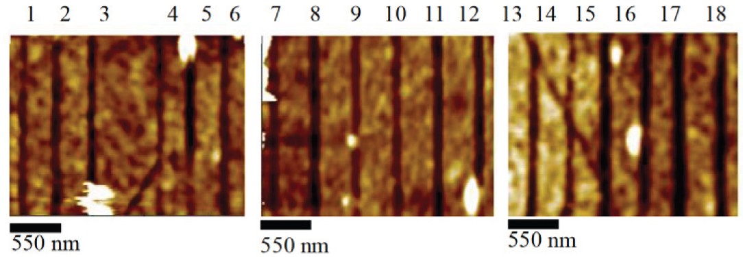
Figure 3. The topology of XY-vibration DOE patterns.
Circular Vibration Expands the Processing Window
Using circular XY vibration, the researchers produced trenches approximately 3.5 to 8 nm deep and 90 to 172 nm wide.
For trench depth, patterning speed produced the strongest statistical effect, followed by voltage and the interaction between voltage and speed. Increasing voltage generally increased the depth of the features, while increasing patterning speed tended to reduce it. This behavior indicates that the time available for the electrically assisted interaction between the probe and material plays an important role in determining how deeply the surface is modified.
Trench width behaved somewhat differently. Voltage was the only parameter identified as having a statistically significant effect on width in the XY-vibration experiment. Higher voltages generally produced wider features, while the effect of speed was less significant.
The circular trajectory also provided an important practical advantage: it enabled successful nanopatterning across a broader range of operating conditions. Combinations of relatively high speed and low voltage that could still produce structures with XY vibration sometimes failed entirely when only Y-axis vibration was used.
The researchers suggest that this difference may arise not only from the additional mechanical motion but also from the way the circular trajectory distributes the electric field along the path of the probe. As a result, circular vibration can enhance material modification and allow pattern formation under conditions that are less effective with reciprocating motion.
Single-Axis Vibration Enables Narrower Features
The Y-axis vibration experiments produced generally smaller features. Measured trench depths ranged from approximately 3.3 to 5.3 nm, while widths ranged from about 55 to 160 nm.
In this configuration, voltage became the dominant factor controlling trench depth. Unlike the XY-vibration results, speed did not show a statistically significant effect on depth over the successfully patterned conditions.
Voltage also had the strongest influence on trench width, although speed contributed significantly as well. Increasing voltage produced wider features, while increasing speed generally reduced their width.
The narrower trenches demonstrate a potential advantage of single-axis vibration when smaller lateral dimensions are required. However, this benefit comes with a more restricted processing window. At the highest tested speed of 1.25 µm/s, low and intermediate voltages frequently failed to produce measurable patterns. Successful patterning at this speed generally required a higher applied voltage.
This suggests that vibration trajectory can be selected according to the desired manufacturing objective. Circular XY vibration provides stronger and more robust material modification, while reciprocating Y-axis vibration can be advantageous when narrower and shallower structures are preferred.
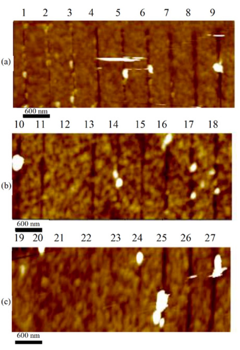
Figure 4. The topology of the patterns with lithography speed of (A) 0.25 μm/s, (B) 0.5 μm/s, and (C) 1.25 μm/s.
Vibration Trajectory Emerges as a Critical Control
To directly compare the two approaches, the researchers combined the experimental datasets and introduced the number of vibration axes as an additional factor in the statistical analysis.
The results showed that vibration axis had the largest statistical effect on both trench depth and width. For depth, the vibration trajectory was followed in importance by voltage and speed. For width, vibration axis again produced the strongest effect, followed by voltage.
This finding highlights an important aspect of vibration-assisted AFM nanomanufacturing: vibration should not be viewed simply as an auxiliary method for reducing machining forces. The geometry of the vibration itself can serve as a fundamental process parameter.
Adding X-axis motion to Y-axis vibration transforms the probe trajectory from reciprocating to circular. This increases lateral interaction with the material and consequently tends to produce wider and deeper structures. At the same time, however, the circular motion improves the ability to generate patterns at higher speeds and lower voltages.
The choice of trajectory therefore introduces a controllable trade-off between feature dimensions and processing capability.
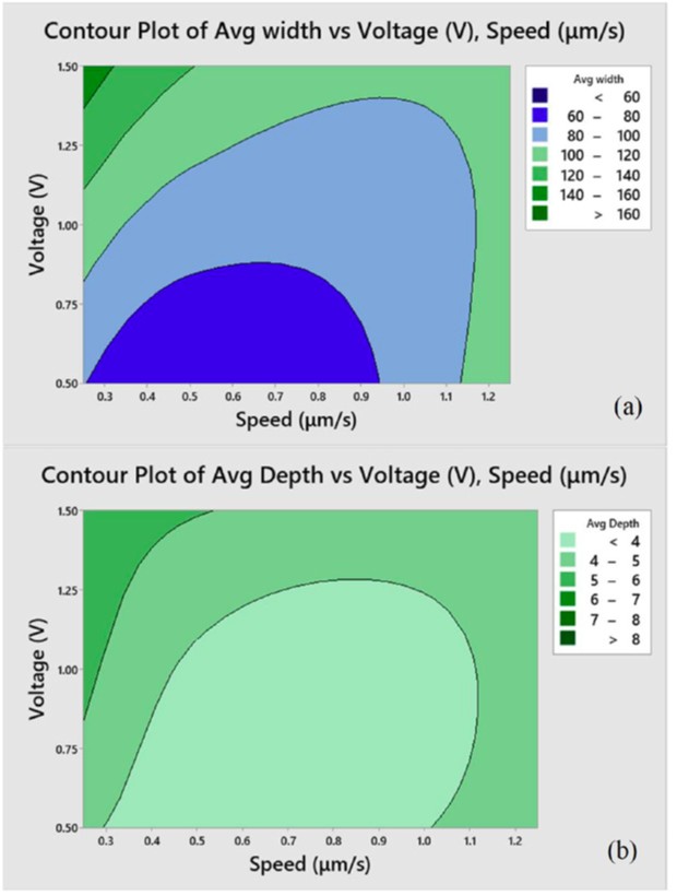
Figure 5. (A) Contour plot of the depth versus the voltage and speed. (B) Contour plot of the width versus the voltage and speed.
Toward More Predictable AFM Nanofabrication
The study demonstrates that combining electric fields with mechanical vibration provides a flexible approach for controlling AFM-based nanopatterning of conductive polymer films. Rather than relying on a single machining parameter, the process can be tuned through the coordinated adjustment of voltage, speed, and vibration trajectory.
For circular XY vibration, voltage primarily controls feature width while speed plays a particularly important role in determining depth. For single-axis Y vibration, voltage becomes the dominant factor for both dimensions. Most significantly, the vibration trajectory itself strongly affects the overall geometry of the resulting structures and determines which combinations of speed and voltage can successfully produce patterns.
These findings provide a clearer framework for selecting AFM nanopatterning conditions according to the desired feature geometry. Applications requiring stronger material modification or a broader operating range may benefit from circular vibration, while single-axis vibration may be better suited to producing narrower and shallower trenches.
More broadly, the work illustrates how AFM can evolve beyond its traditional role as a characterization instrument. By integrating precise probe control with electrical and mechanical excitation, the same fundamental platform used to observe nanoscale surfaces can also be used to manufacture structures on them.
As nanomanufacturing increasingly requires flexible methods for prototyping and fabricating functional materials, such hybrid AFM approaches could provide valuable capabilities for organic electronics, MEMS and NEMS, sensors, and other nanoscale devices where precise control of surface geometry is essential.
NANOscientific Magazine, 2026