Bulk photovoltaic effect in ferroelectric materials
- 03 Jan 2020
- Volume 18
- NanoScientific Magazine, Winter 2020
Zentrum für Innovationskompetenz, Martin Luther Universität Halle-Wittenberg, 06120 Halle (Saale), Germany
 Dr. Akash Bhatnagar
Junior Research Group LeaderLight for High Voltage Photovoltaics, The Centre for Innovation Competence SiLi-nano®, Halle, Germany
The ever-growing demand for renewable energy cannot be overstated. Photovoltaic effect, which involves conversion of light to electricity has been considered as one of the most promising pathways. The field of photovoltaics is largely dominated with the use of semiconductor-based devices. The photovoltaic device primarily consists of a pn-junction with a space charge region at the interface between p- and n-type material [1]. The maximum efficiency obtainable from the pn-junction devices is defined by the Shockley-Quisser limit and has been calculated to be around 30% [2]. The innate limitation of the photovoltaic energy conversion in semiconductors
has triggered the pursuit to find new materials that have a fundamentally different mechanism for charge separation.
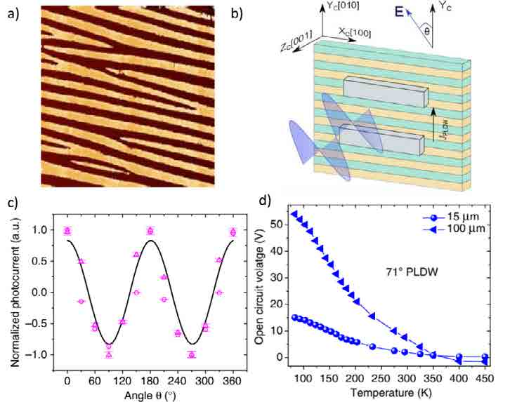
Figure 1. (a) Piezo force microscope 3.5 x 3.5 µm2 image acquired with Park XE-100. The brown and yellow colors show different ferroelectric domains. (b) Measurement geometry for BPV effect. (c) Angular dependent photovoltaic current. (d) Enhancement in Voc as the temperature is reduced in the case of 71° domains measured across 15 and 100 µm gaps [Taken from 4]
In this context, the photovoltaic effect in ferroelectric materials, i.e.
bulk photovoltaic effect (BPV), has attracted a lot of attention. Ferroelectric materials can exist in different states of polarizations, or domains (Figure 1a), and can be switched from one state to the other by the application of electric field. The region in between the two domains is referred to as the domain wall. The photovoltaic effect in these materials is driven by the symmetry of the material rather a junction. As a result, the photocurrent generated is determined by a tensor which is largely analogous to the piezoelectric tensor of the material [3]. The photocurrent when measured with a linearly polarized light (Figure 1b), exhibits a dependency on the angle which the electric field of linearly polarized light makes with the direction of current flow (Figure 1c). Interestingly, the resultant open circuit voltages (Voc) are much higher than the band gap of the material and are in the range of 10–20V! Even higher voltages can be achieved if the overall conductivity of the samples is suppressed by lowering the temperature (Figure 1d) [4].
Another interesting aspect is the switch-ability of the effect. Unlike semiconductor-based photoeffect, the direction of photocurrent can be effectively reversed and under certain conditions the magnitude can be massively reduced (Figure 2). Such tunability arises from the ordering of domains which can manipulated by the application of electric field. Conversely, the BPV effect can be also utilized to determine the ordering of domains and estimate the net polarization.
However, there are some severe drawbacks that need to be addressed to
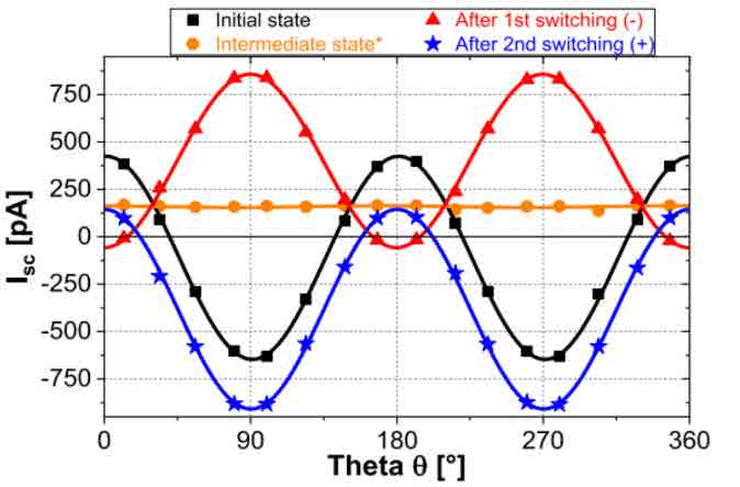
Figure 2. Photovoltaic current measured after each step of domain rearrangement upon application of switching field [Taken from 5].
widen the applicability of BPV effect. For instance, the band gap of ferroelectric material is typically above 2.8 eV, due to which only a small fraction of solar spectra can be utilized. Also, the current densities reported until now are way too low for any meaningful application. Nevertheless, with rapid development in thin film deposition and computational techniques, new material systems can be proposed and realized which would be able to overcome such limitations.
References:
1) Sze, S.M. (1981) Physics of semiconductor devices, John Wiley & Sons, INC
2) Shockley, W., and Queisser, H.J. (1961) Detailed balance limit of efficiency of p-n junction solar cells. J. Appl. Phys., 32 (3), 510–519.
3) Belinicher, V.I., Malinovskii, V.K., and Sturman, B.I. (1977). Photogalvanic effect in a crystal with polar axis. Soviet Physics – JETP 46 (2): 362–366
4) Bhatnagar, A., Roy Chaudhuri, A., Heon Kim, Y. et al. (2013). Role of domain walls in the abnormal photovoltaic effect in BiFeO3. Nature Communications 4 (May): 2835.
5) Knoche, D.S., Yun, Y., Ramakrishnegowda, N. et al. Domain and Switching Control of the Bulk Photovoltaic Effect in Epitaxial BiFeO3 Thin Films. Sci Rep 9, 13979 (2019)
FEI HUI, A POSTDOCTORAL FELLOW AT TECHNION-ISRAEL INSTITUTE OF TECHNOLOGY ANNOUNCED ASPARK AFM SCHOLAR
Abstract: Scanning probe microscopy for advanced nanoelectronics
As the size of electronic devices continues to shrink, characterization methods capable of precisely probing localized properties become increasingly important. Scanning probe microscopy techniques can examine local phenomena, and conductive atomic force microscopy can, in particular, study local electromechanical properties. Such techniques have already played a valuable role in the development of nanoelectronics, but their capabilities remain relatively limited compared with the probe stations typically used to examine electronic devices. Here, we discuss the potential of conductive atomic force microscopy in nanoelectronics. We explore possible characterization strategies, enhanced electronics for the technique and improved multiprobe approaches. We also propose a multiprobe scanning probe microscopy system that combines different types of probes and could allow multiple nanofabrication and characterizationexperiments to be carried out simultaneously under vacuum conditions.
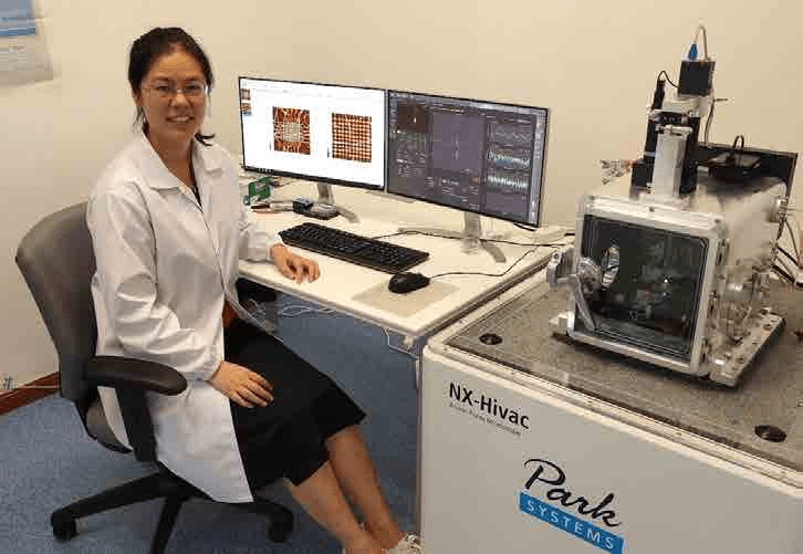
Dr. Fei Hui at the AFM (Park NX-Hivac) lab
Fei Hui is currently a postdoctoral fellow at Technion-Israel Institute of Technology. She received her doctoral degree from the University of Barcelona in 2018. During her PhD, Dr. Hui was a visiting scholar at Massachusetts Institute of Technology (USA) for 12 months, where she learned chemical vapor deposition of two-dimensional (2D) materials (e.g. hexagonal boron nitride, graphene) on different substrates (i.e. Cu, Pt, Fe and Ni). She also received the Researcher Mobility Grant from the Royal Society of Chemistry, which supported her studies at the University of Cambridge (UK) for 6 months. In the Cambridge Graphene Center, she learned how to synthesize graphene oxide thin films and, more interestingly, how to cover nanoprobes with thin films of this material via spray technique. She has published over 40 research papers (11 papers are as first-author) in top journals including Nature Electronic, Advanced Functional Materials, ACS Applied Materials and Interfaces, and 2D Materials (amongothers), and has more than 811 citations indicated by Google Scholar (https://scholar.google.com/. She has applied for two international patents, and one of them (cost-effective fabrication of ultradurablegraphene coated nanoprobes) attracted aroundapproximately $1 million investmentworth of investments.
Please summarize the research you do and explain why it is significant?
My research topic is the development of two-dimensional (2D) materials based electronic devices. We are aiming to integrate 2D materials (e.g. hexagonal boron nitride, graphene or molybdenum disulfide) into electronic devices (e.g. memristors or field effect transistors). Due to the atomic thin layer and extraordinary properties (e.g. high thermal and electrical conductivity, flexibility and transparency) of 2D materials, it allows us to design miniaturized devices, which exhibit some exotic performances that conventional transition metal oxides (e.g. HfO2)-based devices do not show. More specifically, I first synthesized monolayer or multilayer 2D materials using chemical vapor deposition (CVD) methodology. After growth I used several techniques to analyze the quality of these materials, mainly Raman Spectroscopy and cross-sectional transmission electron microscopy (X-TEM), but the technique that provided me best results was conductive atomic force microscopy (CAFM). Using this technique, I explored the dielectric properties of hexagonal boron nitride (h-BN) and graphene oxide (GO), including tunneling current, charge trapping, trap-assisted tunneling, stress induced leakage current, dielectric breakdown and resistive switching (RS). I also used these 2D materials to fabricate memristive devices, and analyzed them using a probe station connected to a semiconductor parameter analyzer (working in different atmospheres).
How might your research be used?
In my work, I employed a scalable CVD technique to synthesis large sizes of 2D materials, which allow us to fabricate high-yield electronic devices and study their device-to-device variability. Moreover, this methodology is more compatible with and useful for the industry than single/few devices fabricated by mechanical exfoliation. In our previous work, we have proved that h-BN can be used as a RS medium and the metal/h-BN/metal devices showed both volatile and non-volatile RS behaviors, enabling the emulation of a range of synaptic-like behavior, including both short- and long- term plasticity. Therefore, our research would accelerate the use of 2D materials for building future wafer-scale and high-density electronic memories and/or artificial neural networks.
What features of Park AFM are the most beneficial and why?
The Park AFM system is a powerful tool that provides us with more accurate and reliable information under different conditions (ambient and vacuum conditions), which is extremely important for the research field of nanoscience. First of all, the true non-contact mode allows us to acquire the topographic information, such as
the wrinkles of 2D materials or some tiny particles, without the damage of probes and surface modification of specimens. Second, the image/position drift is negligible, we can perform spectroscopy measurements (e.g. current vs. voltage, force vs. distance) at specific locations or in a matrix pattern and then go back to them exactly. Moreover, the navigation and the software interface are quite user-friendly, which save us much more time.
Why is the Park AFM important for your research?
This Park NX-Hivac system is able to simultaneously perform four tasks that are essential to study RS reliably:This Park NX-Hivac system is able to simultaneously perform four tasks that are essential to study RS reliably: i) measure currents in tapping mode (to avoid premature tip wearing and material damage); ii) measure high currents from picoamperes to milliamperes in both polarities by using a logarithmic preamplifier (to monitor the set/reset transitions in situ); iii) measure in high vacuum up to 10-6 torr (to avoid local anodic oxidation and unwanted moisture-related reactions); and, iv) measure at high temperatures up to 600 ºC (not only to study reliability, but also to evaporate all water molecules on the materials after pumping the vacuum). The need of these four features to reliably measure RS at the nanoscale is extensively described in the book (Conductive Atomic Force Microscopy: Applications in Nanomaterials, ISBN: 978-3-527-69978-0, Wiley-VCH Weinheim, Germany, 2017) edited by Prof. Mario Lanza, who is a leading expert in CAFM science, and there is no other equipment in the world that can carry out all these actions.simultaneously. The use of this tool will be a high advantage compared to other groups.
