Characterization of 2D materials by imaging spectroscopic ellipsometry (ISE)
- 31 May 2023
- Volume 24
- NANOscientific Magazine, Spring 2023
Introduction
2D materials, which have the potential to revolutionize entire areas of technology, require decisive tasks to advance developments quickly and efficiently. These tasks include the targeted finding of suitable candidates, as well as fast and efficient quality control of technically manufactured 2D materials. Many scientists especially see applications in the field of micro photonics, lighting, imaging, and sensors. For this range of applications, detailed knowledge of the optical properties is essential, especially to the samples depending on their thickness. Imaging Spectroscopic Ellipsometry (ISE) is a single device that combines the benefits of spectroscopic ellipsometry and optical microscopy (Figure 1a). The combination of these two technologies creates a unique metrology tool that redefines the limits of both ellipsometric measurements and polarization-contrast microscopy. The enhanced spatial resolution of imaging ellipsometers (down to 1 µm) expands ellipsometry into new areas of microanalysis, microelectronics, and bioanalytics. ISE is an all-optical, non-contact metrology technique that excels in the layerthickness and material characterization of micro-structured thin-film samples and substrates. The microscopic part allows for a simultaneous measurement of all structures within the field of view of the optical system (Figure 1b). The lateral resolution is defined by the ability of the microscopic part to distinguish details of a specimen or sample, not by the spot size of the illumination beam as in conventional spectroscopic ellipsometry. This provides the benefit of lateral resolution and the capability to use each pixel of the camera as a single detector. Additionally, the detector always offers a live image (ellipsometric contrast micrograph) of the sample, even during the measurement.
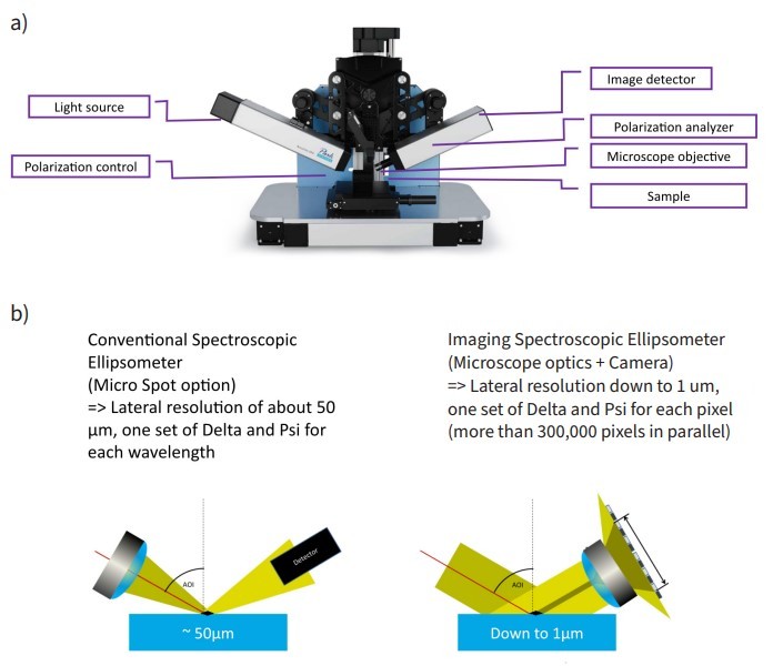
Figure 1. Imaging Spectroscopic Ellipsometer Accurion EP4 (Park Systems GmbH) (a) Basic concept of Conventional Spectroscopic Ellipsometer vs. Imaging Spectroscopic Ellipsometer (b).
In technical applications, the thickness of a sheet or plate is typically measured using a caliper. To improve the precision of such measurements, a Vernier scale is often employed. In essence, an ellipsometer can be thought of as a Vernier scale for the nano-scale world, with the elliptical polarization state providing a greater degree of accuracy for very thin films – similar to the way in which a Vernier scale is used in macroscopic settings. An imaging ellipsometer merges this thin film metrology tool with microscopic imaging, mapping, and the characterization of microscopic thin films like 2D materials. The ellipsometric configuration of the Accurion EP4 involves a Polarizer Compensator Sample Analyzer (PCSA), with all optical components being motordriven. By adjusting the orientation of one or more optical components, the contrast can be optimized (as shown in Figure 2a), such as between the substrate and a monolayer or between stacks with different layer numbers [1]. Wurstbauer et al. [2010] also demonstrated the ability to optimize contrast between either graphene and substrate or between substrate and impurities from the tape used in exfoliation [2].
Ellipsometric contrast micrographs: Fast, non-contact, wafer-scale, atomic layer resolved imaging with tunable contrast
In general, ellipsometric contrast micrographs (ECM) enable an atomic layer resolved, quantitative mapping of chemical vapour deposited graphene layers on Si/SiO2 -wafers, but also on rough Cu catalyst foils (Figure 2b). Braeuninger-Weimeret al. [2018] highlight that ECM is applicable to all application relevant substrates and discuss the optimization of ECM parameters for high throughput characterization. Furthermore, they show ECM of monolayer hexagonal BN (h-BN) and of h-BN/ graphene bilayers, highlighting that ECM is applicable to a wide range of 2D layered structures that have been very challenging to characterize before [1].
The shape of an ellipse is defined by Delta and Psi
Ellipsometry deals with elliptic polarized light (Figure 3a) that can be described by the ellipsometric angles Delta and Psi (Figure 3b). Braeuninger- Weimar et al. showed that an even better distinction between the different numbers of layers can be achieved with microscopic delta maps [1]. From the point of view of thin film metrology, it is important that these angles are related by the Drude equation (Figure 3c) with the reflection coefficients of the sample surface. To translate the measured data into physical meaningful parameters like layer thickness of thin films or refractive index of a material, a comparison by a liberation process of the measured data with simulated data is required (optical modelling).
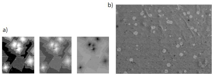
Figure 2. Ellipsometric Contrast Micrographs (ECM) of CVD-Graphene Si/SiO2 wafers - tunable contrast through changed orientation of the optical components (a) and a stitched super image of graphene directly on copper- 15x10 mm (b).
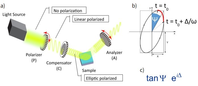
Figure 3. Change of the state of polarization on the pathway of light of an ellipsometer (a) [3], [4] and how the shape of an ellipse is described by the ellipsometric angles Delta and Psi (b) and Drude equation (c).
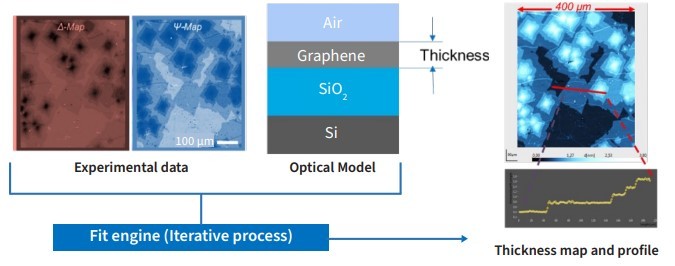
Figure 4. Microscopic mapping of Delta and Psi for film thickness mapping and profiling.
Automated search of flakes of monoor n-layers of 2D-materials
The aforementioned capability of ECM and Delta-maps to identify samples of specific layer numbers can automatically localize regions of desired thicknesses, such as monolayers or bilayers on any substrate [5]. This process is a promising first step in a cascade of characterization methods from macro to nano. The visualization of defects and grain boundaries in large-area graphene coatings using an ECM/Delta mapsbased QC approach, in combination with complementary technologies like atomic force microscopy (AFM) and magnetic force microscopy (MFM), is especially promising.
Micro Ellipsometry versus Microscopic
The capability of imaging ellipsometry can be explained by using two borderline cases. The first method is micro ellipsometry, where optical thin-film metrology is based on so-called regions of interest (ROI). These ROIs are set to select the camera pixels that are averaged for the measurement. The second method is microscopic mapping, which involves determining parallel values for all the pixels, thereby enabling the determination of a layer thickness map or distribution.
Optical dispersion of 2D-Materials
Let's examine the spectroscopic ability of ISE in more detail: The main goal of spectroscopic ellipsometry measurements for 2D materials is to determine the optical characteristics of the flakes. The acquired data involves comparing the sets of delta and Psi measurements (for each ROI or even per pixel) with calculated values of an optical model through an iterative process. The calculation is founded on the overall layer structure. The optical properties of the substrate are predetermined or preferably, determined simultaneously - a standard technique in the characterization of 2D materials using an imaging ellipsometer. In the literature, optical dispersion detection based on ISE has been reported for various materials, including graphene [6], graphene oxide [7], graphene embedded in h-BN [8], 2D-MoS2 [9],[10], 2D-MoO3 [11], and TCM-heterostructure [12] – just to name a few. The next step could be determining the shape, size, and symmetry of these materials depending on their optical properties [13]. For a more general outlook on future limitations and requirements, please refer to the paper titled "Imaging ellipsometry for structured and plasmonic materials" [14].
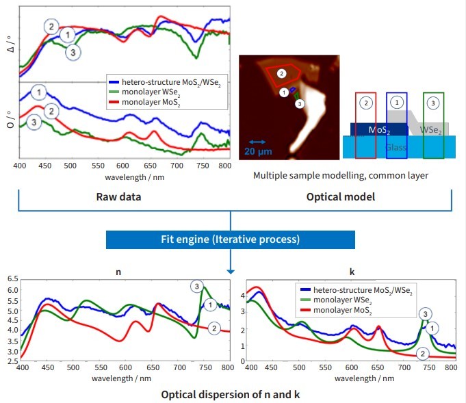
Figure 5. Micro ellipsometry of a heterostructure of 2D-materials using different regions of interest (ROI) in parallel (1),(2),(3).
Operando Imaging Spectroscopic Ellipsometry
Over the past few years, several papers have been published on operando imaging ellipsometry [15] and operando imaging spectroscopic ellipsometry [16] of graphene-based samples. The key aspect is that imaging ellipsometry can detect changes in the thin film material during processes. For instance, it can track the intercalation of sodium ions depending on the voltage.
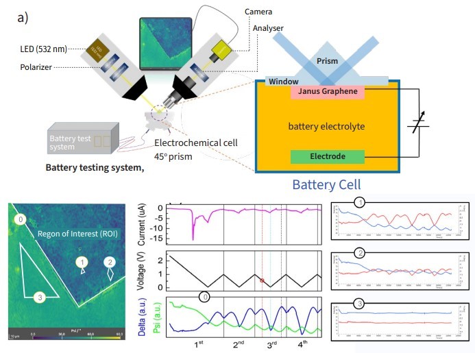
Figure 6. Setup for in situ operando imaging ellipsometry to follow the intercalation of sodium ions into Janos graphene [15].
Conclusion
In conclusion, Imaging Spectroscopic Ellipsometry (ISE) proves to be a powerful tool for the characterization of 2D materials, filling an important gap in 2D metrology. It can be utilized to measure the thickness of monolayers, as well as the optical properties of 2D materials. Additionally, it is applicable for measuring heterostructures and small devices, as well as identifying defects and wrinkles in the flakes. Moreover, it can measure the optical properties of 2D materials on various substrates, making Imaging Ellipsometry a valuable tool for the characterization of 2D materials.
References:
[1] Braeuninger-Weimer, P., Funke, S., Wang, R., Thiesen, P., Tasche, D., Viöl, W., & Hofmann, S. (2018). Fast, noncontact, wafer-scale, atomic layer resolved imaging of two-dimensional materials by ellipsometric contrast micrography. Acs Nano, 12(8), 8555-8563.
[2] Wurstbauer, U., Röling, C., Wurstbauer, U., Wegscheider, W., Vaupel, M., Thiesen, P. H., & Weiss, D. (2010). Imaging ellipsometry of graphene. Applied Physics Letters, 97(23), 231901.
[3] Operation Manual EP4, Park systems
[4] Tompkins, H., & Irene, E. A. (2005). Handbook of ellipsometry. William Andrew. [5] Funke, S., Wurstbauer, U., Miller, B., Matković, A., Green, A., Diebold, A., ... & Thiesen, P. H. (2017). Spectroscopic imaging ellipsometry for automated search of flakes of mono-and n-layers of 2D-materials. Applied Surface Science, 421, 435-439.
[6] Matković, A., Beltaos, A., Milićević, M., Ralević, U., Vasić, B., Jovanović, D., & Gajić, R. (2012). Spectroscopic imaging ellipsometry and Fano resonance modeling of graphene. Journal of Applied Physics, 112(12), 123523.
[7] Jung, I., Vaupel, M., Pelton, M., Piner, R., Dikin, D. A., Stankovich, S., ... & Ruoff, R. S. (2008). Characterization of thermally reduced graphene oxide by imaging ellipsometry. The Journal of Physical Chemistry C, 112(23), 8499-8506.
[8] Toksumakov, A. N., Ermolaev, G. A., Tatmyshevskiy, M. K., Klishin, Y. A., Slavich, A. S., Begichev, I. V., ... & Ghazaryan, D. A. (2023). Anomalous optical response of graphene on hexagonal boron nitride substrates. Communications Physics, 6(1), 13.
[9] Funke, S., Miller, B., Parzinger, E., Thiesen, P., Holleitner, A. W., & Wurstbauer, U. (2016). Imaging spectroscopic ellipsometry of MoS2. Journal of Physics: Condensed Matter, 28(38), 385301.
[10] Ermolaev, G.A., Stebunov, Y.V., Vyshnevyy, A.A. et al. (2020) Broadband optical properties of monolayer and bulk MoS2. npj 2D Mater Appl 4, 21 (2020). https://doi.org/10.1038/s41699-020-0155-x
[11] Andres-Penares, D., Brotons-Gisbert, M., Bonato, C., Sánchez-Royo, J. F., & Gerardot, B. D. (2021). Optical and dielectric properties of MoO3 nanosheets for van der Waals heterostructures. Applied Physics Letters, 119(22), 223104.
[12] Sigger, F., Lambers, H., Nisi, K., Klein, J., Saigal, N., Holleitner, A. W., & Wurstbauer, U. (2022). Spectroscopic imaging ellipsometry of two-dimensional TMDC heterostructures. Applied Physics Letters, 121(7), 071102.
[13] Magnozzi, M., Pflug, T., Ferrera, M., Pace, S., Ramó, L., Olbrich, M., ... & Canepa, M. (2021). Local optical properties in CVDgrown monolayer WS2 flakes. The Journal of Physical Chemistry C, 125(29), 16059-16065.
[14] Hingerl, Kurt. "Imaging ellipsometry for structured and plasmonic materials." Journal of Applied Physics 129.11 (2021): 113101.
[15] Sun, J., Sadd, M., Edenborg, P., Grönbeck, H., Thiesen, P. H., Xia, Z., ... & Palermo, V. (2021). Real-time imaging of Na+ reversible intercalation in “Janus” graphene stacks for battery applications. Science advances, 7(22), eabf0812.
[16] Okano, S., Sharma, A., Ortmann, F., Nishimura, A., Günther, C., Gordan, O. D., ... & Zahn, D. R. (2020). Voltage-controlled dielectric function of bilayer graphene. Advanced optical materials, 8(20), 2000861.
