Park AFM Scholarship Awards - Xin Yin
- 11 Oct 2017
- Volume 11
- NanoScientific Magazine, Fall 2017

Phd Candidate In The Department Of Materials Science And Engineering At University Of Wisconsin-Madison
“PARK AFM PROVIDES US WITH A HIGH-RESOLUTION AND RELIABLE MEASUREMENT OF THE THICKNESS AT THE SUB-NANOMETER LEVEL.”
Xin Yin is currently a PhD candidate in the department of Materials Science and Engineering at University of Wisconsin-Madison. He joined Professor Xudong Wang's group in 2012. His research interests include study of growth kinetics in various ZnO nanostructures, and synthesis and electronic properties of nanometer-thick 2D ZnO nanosheets.
1. Summarize the research you are doing and explain briefly how it will impact society. Why is your research important?
Two-dimensional (2D) nanomaterials, with just one or a few atomic layers, exhibit physical properties dissimilar to those of their bulk counterparts. However, the current 2D materials have been largely limited to naturally layered materials, like graphene and transition metal dichalcogenides.
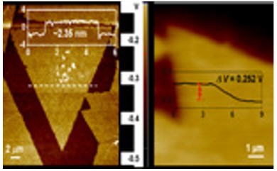
My research mainly focuses on the growth of two dimensionalnon-layered materials. With a unique growth method, single-crystalline nanometer-thick ZnO nanosheets with the size up to 20 micrometers are realized at water-air interface with surfactant monolayer as a template. More importantly, the thickness of ZnO nanosheets could be tuned from one unit cell to four unit cells.
This is the first time to realize the growth of ultrathin ZnO nanosheets. On one hand, it provides an opportunity to study the electronic, photonic, and mechanical properties emerging from the ultrathin feature of ZnO. For example, our investigation has found that the work function shows monoclinic increase with nanosheet thickness. This thicknessdependent work function provides a good flexibility in designing heterojunctions withtunable band alignment. On the other hand, the research presents a strategy to boost the abundance of 2D materials through applying the unique growth method to other material systems.
2. What is the most useful part of using Park AFM for your research? Please explain what features are most useful and why?
Since we focus on the synthesis of 2D nanomaterials, the characterization on the thickness of the nanosheets is important. Park AFM provides us with a high-resolution and reliable measurement of the thickness at the sub-nanometer level. Moreover, to locate at one specific position for the measurement of electrical properties, as well as the mapping measurement, such as the surface potential mapping and current mapping, provides a chance to recognize and investigate the property difference from point to point.

