The Role of Nanoscale Technologies in Semiconductor’s Next Stage in Evolutionary Breakthroughs
- 01 May 2015
- Volume 4
- NanoScientific Magazine, Spring 2015

Phil Kaszuba is an Advisory Engineer/ Scientist for IBM’s Systems and Technology Group. He currently directs the Scanning Probe Microscopy Laboratory in the Analytical Services organization at IBM’s Essex Junction, Vermont semiconductor fabrication facility. He holds a B.S.E.E. from the University of Vermont with a concentration in semiconductor device physics. His work is centered on applied SPM for nanoscale semiconductor technology analysis and nanoinstrumentation development. Having worked in SPM for 23 years, Phil is a recognized expert in the field and one of the foremost authorities in applied SPM for nanoscale semiconductor technology analysis. Phil was involved with the initial development of many of the SPM based analytical techniques and instruments used in the semiconductor industry today. He is currently developing new SPM based analytical techniques for applications in nanoscale semiconductor technology development, fabrication line monitoring, device characterization, and failure analysis. Phil has authored numerous articles and papers including invited speaking engagements at universities, industry seminars, and classroom instruction. He holds a number of U.S. and international patents in the field of Scanning Probe Microscopy. Included in his portfolio are the patents for the Scanning Surface Photo Voltage Microscope (SSPVM) and Silicided Silicon Conductive Tips. Phil is a member of the Electronic Device Failure Analysis Society. He serves regularly as a review panel member for the National Science Foundation and a technical advisor to the Defense Advanced Research Projects Agency (DARPA). Phil is also a 15 year committee chair veteran and contributing author to the International Symposium for Testing and Failure Analysis.
Phil Kaszuba who currently directs the Scanning Probe Microscopy Laboratory at IBM is an active user of Park Systems AFM, the industry's leading atomic force microscope for Semiconductor Defect Review and microscopy analysis.
With the growing complexity of new processes and introduction of new materials the needs for product yield management and process control are placing unprecedented demands on failure analysis laboratories in the semiconductor industry. These demands are calling for faster and superior analytical capabilities to determine root cause failure mechanisms in semiconductor devices fabricated using deep sub-micron processes. The Scanning Probe Microscope (SPM) is an analytical instrument used in root cause failure analysis. Scanning Capacitance Microscopy is a SPM technique that maps the dopant profile of a semiconductor device while simultaneously obtaining a topographic image. Using constantly evolving and newly developed techniques a plethora of physical, electrical, and chemical properties of a sample may be routinely analyzed. AFM has become a mainstay technique for metrology applications especially in manufacturing line monitoring for critical dimension analysis and patterned structure sidewall analysis.

You have been in the field of Scanning Probe Microscopy (SPM) for over 23 years and worked with one of the first AFMs at IBM. What have been the major milestones as the industry advanced into nanoscale microscopy?
Working with a prototype AFM in the early 90’s was dramatically different than the SPMs of today. Virtually all of the system set up was performed manually using racks of discrete electronic equipment and a laser interferometer. Typical set up time was 1-2 hours. Analytical techniques were largely limited to non-contact Atomic Force Microscopy (which sensed the van der Waals attractive force between the tip and sample surface) and Scanning Kelvin Probe Microscopy (SKPM). Resolution was adequate for semiconductor device sizes of the era. With current systems, the discrete electronics (which once took up half of a room) have been consolidated into a unit the size of a desktop computer, the interferometer and optical bench have been replaced by a laser diode/photo detector, and system controls are facilitated with software. Set up time can be as little as 10 minutes. Using constantly evolving and newly developed techniques a plethora of physical, electrical, and chemical properties of a sample may be routinely analyzed. Additionally, advancements in probe technology have enabled nanometer to sub nanometer resolution for various techniques. In this interview, Phil explains how new advances in the evolving Semiconductor at increasing nanoscale is creating frontier science in medicine, energy and space exploration that greatly impact each of us and our environment.
How does Scanning Probe Microscopy (SPM) help to make semiconductor devices smaller, faster and use less power?
In the semiconductor industry, the evolution of each new technology node is driven by three primary objectives: devices need to be smaller, faster, and use less power. Consider the amount of data storage, control, or computing power available now in the personal electronic devices that fit in our pocket. The technology to build such devices was enabled by rapid evolutionary advances in the semiconductor industry with SPM providing invaluable data from research to development to production. Critical to the successful development of each new technology is a thorough understanding of the basic circuit elements that are combined to comprise functional electronic devices. Prior to the development of applied SPM techniques, researchers and development engineers relied heavily on technology simulation algorithms to aid them in understanding device performance and fabrication process development. AFM, SKPM and Scanning Capacitance Microscopy (SCM) analyses have provided empirical data that reflects the true outcome of a device design or fabrication process, and how that translates into smaller, faster, and more efficient.
Why is topographical information so important in semiconductor manufacturing and failure analysis?
Devices continue to get smaller in all three dimensions with the introduction of each new technology node. Consequentially, it has become increasingly important to fully understand the physical morphology of silicon substrates as well as the numerous films that are grown or deposited and patterned in the fabrication of functional electronic devices. Displacements of atoms from the normal crystal lattice are commonplace and such a displacement in a silicon substrate, as little as a single atomic plane can cause catastrophic failure if it occurs in the wrong place. AFM can routinely reveal such single plane displacements as well as other detrimental features in a non-destructive fashion. Understanding film roughness has become critically important, especially after Chemical-Mechanical Polishing (CMP) and gate dielectric growth steps. Using appropriate post processing algorithms, high resolution AFM topographic data can be used to ‘quantify’ the physical characteristics of a film or layer after such processing steps using industry standard metrics. Lastly AFM has become a mainstay technique for metrology applications especially in manufacturing line monitoring for critical dimension analysis and patterned structure sidewall analysis.
What has been the most important contribution of Scanning Probe Microscopes to the semiconductor manufacturers?
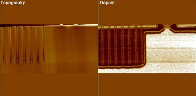
To gain a good understanding of SPM’s most significant contribution to the semiconductor industry let’s first look at some of the fundamental fabrication steps of semiconductor devices. Purified silicon is grown into single crystal silicon, processed into ‘wafers’ and rendered conductive in very specific areas through the implantation of atomic impurities or ‘dopants’. Proper placement of dopant atoms (in all 3 dimensions) in single crystal silicon is the foundation for fabricating semiconductor circuit elements such as transistors, diodes, resistors, and capacitors. Scanning Capacitance Microscopy (SCM) has been the single most important scanning probe analytical technique to the industry because with SCM it becomes possible to accurately detect (with nanometer resolution) the position, distribution, and relative concentration of dopant atoms in silicon. Prior to the availability of SCM there was no practical analytical method that could show dopant distribution across a complete structure.
Can you explain how you analyze dopant profiles in silicon semiconductor devices?
As mentioned previously, specific dopants are implanted into select areas in the silicon to alter their conductivity. It is important that after implantation, the dopants are rendered electrically active by annealing the implanted silicon at a high enough temperature for a requisite period of time. Depending on the dopant species there will either be a net excess of electrons (n-type) or shortage of electrons (p-type) in the implanted areas. A charge carrier in n-type silicon is called simply an ‘electron’ and in p-type type silicon the electron void that moves throughout is called a ‘hole’. Dopant concentrations determine the level of electrical conductivity. SCM is a technique that uses an externally applied electrical stimulus to move these carriers. This controlled carrier motion is sensed by the SCM probe which is in contact with the silicon surface which has been lightly oxidized. Knowing the magnitude and polarity of the applied bias along with the carrier response it is straightforward to determine the dopant polarity and relative concentration of the area being analyzed. Raster scanning the probe throughout an area of interest yields a map of the dopant type and relative concentration for a given area. Nanometer resolution has been achieved using the latest in SCM probe technology. This has been, and continues to be the “workhorse” technique for transistor dopant analysis since refinement of the technique in the early 90’s.
What are the next steps in the evolution of nanoscale technologies as they apply to the Semiconductor industry?
The semiconductor industry has followed a very aggressive roadmap as it transitions to each new technology node. Technologies evolved from 45nm to 32nm to 22nm quite rapidly and this evolution involved not only shrinking device geometries dimensionally, but the introduction of novel materials in order to address issues that arose from building transistors with channel lengths that are a mere 40 atoms long and dielectrics a few molecules in thickness . The next major step for the industry is the transition from 22nm to 14 nm which has seen a major redesign of the basic transistor. After 14nm we move on to 10nm followed by 7nm! SPM provides critical data in the analysis of devices at each of these technology nodes from basic research to full production.
What new materials are being researched currently? have been developed recently?
The fundamental circuit element in integrated circuits is the Field Effect Transistor (FET). The basic FET structure is comprised of doped regions of silicon onto which a thin “gate dielectric” is grown. A conductive stripe or “gate” is deposited on the gate dielectric to turn the FET on and off. The most critical film in this ‘stack’ is the gate dielectric which had traditionally been SiO2 that was typically tens of angstroms in thickness. As technologies progressed and dimensions shrunk, this film was made thinner and thinner to the point where it was only a few molecular layers in thickness. Quantum tunneling effects between the gate and substrate became a concern so it was therefore necessary to modify the dielectric to alleviate this problem. Incorporating Hafnium into the gate dielectric increases the dielectric constant thereby solving this scaling problem. The implementation of HfO2 was probably the single biggest recent breakthrough in planar FET technology.
How is Conductive AFM (C-AFM) used to locate molecular contaminants and why is this important?
As FET gate dielectric layers continued to thin it became evident that molecular contaminants in this insulating layer between the gate and substrate could readily compromise device functionality. With millions of FETs on a chip it is likely that this will occur sporadically and it is therefore important to have a thorough understanding of gate dielectrics. C-AFM is an electrical method that has the ability to map current flow properties through a sample with nanometer resolution and femtoamp sensitivity. C-AFM has proven to be an invaluable technique in localizing even the most subtle of electrical inhomogeneities in that most critical layer; the gate dielectric. A dielectric film may be analyzed ‘as grown’ or on a fully constructed FET. In the case of a fully constructed FET, the device must be de-constructed using a combination of mechanical and chemical steps to essentially reverse the fabrication process until the layer of interest, i.e., the gate dielectric, is exposed. It is first inspected using AFM at high resolution using a standard silicon probe to determine whether there are any obvious topographic anomalies. Then C-AFM is used, starting at a low level of applied DC bias. An image is captured and then the process is repeated, increasing the bias with each image in the sequence until either of the following occurs: A localized ‘spot’ of current flow appears indicating a local variation in dielectric strength….or….low level tunneling current begins to appear in multiple locations across the dielectric surface; this is normal for a good, uniform dielectric. When a small discrete spot is found, other techniques (SKPM, TEM, AFM) may then be used to understand the cause for the local variation in dielectric strength.

"THE SCANNING PROBE MICROSCOPE HAS PLAYED A VITAL ROLE THROUGH PROVIDING CRITICAL DATA IN SUPPORT OF THE EVOLUTION OF EACH NEW SEMICONDUCTOR TECHNOLOGY NODE AS DEVICES GEOMETRIES APPROACH A MOLECULAR SCALE. THE SEMICONDUCTOR INDUSTRY HAS TAKEN ON AN AGGRESSIVE PATH IN DEVELOPING EMERGING TECHNOLOGIES AND APPLICATIONS ENABLING CAPABILITIES SUCH AS CONTROLLING EVERY HOME APPLIANCE, FROM ANY LOCATION, WITH A SIMPLE HANDHELD DEVICE, AUTOMOBILES THAT MANEUVER THEMSELVES, AND MACHINES THAT HAVE THAT CAPABILITY TO "THINK" AND EVEN WIN AT "JEOPARDY!".
Continued advancements in semiconductors will enable faster medical diagnoses, better understanding of diseases and their cures, rapid development and deployment of pharmaceuticals through simulation of chemical, physical, and biological processes and exploration of our solar system from Mars and beyond, to the far reaches of the universe. Solutions to the planet's insatiable demand for energy could be realized through understanding and learning to safely harvest the immense power available from atomic interactions by running massive computer simulations. Semiconductor industry breakthroughs will aid in the creation of prosthetics that adapt seamlessly and function identically to original human body parts. The list is only limited by the ingenuity and creativity of today's scientists and the Scanning Probe Microscope will have an increasingly more important role as an analytical instrument in the realms of research, development, and manufacturing."
What are the future technological advances that you think might come from semiconductor SPM research?
The Scanning Probe Microscope has played a vital role in support of the evolution of each new semiconductor technology node through providing critical and in some cases previously unavailable data as device geometries approach a molecular scale. The semiconductor industry has taken on an aggressive path in developing emerging technologies and applications enabling end user capabilities such as controlling every home appliance, from any location with a simple handheld personal electronic device, automobiles that maneuver themselves, and massively complex machines that have that capability to "think" and even win at "Jeopardy!". Continued advancements in semiconductors will enable faster medical research, rapid, accurate diagnoses, better understanding of diseases, their causes, and their cures, and rapid development and deployment of pharmaceuticals through simulation of chemical, physical, and biological processes. Forthcoming is even more detailed exploration and understanding of our solar system starting with a manned expedition to Mars and someday beyond; ultimately to the distant reaches of the universe. Solutions to the planet's insatiable demand for energy could be realized through understanding and learning to safely harvest the immense power available from atomic interactions by running massive computer simulations. Semiconductor industry breakthroughs will aid in the creation of prosthetics that adapt seamlessly and function identically to original human body parts. The list is only limited by the ingenuity and creativity of today's scientists and the Scanning Probe Microscope will continue to have an increasingly more important role as an analytical instrument in the realms of research, development, and manufacturing.