Nanoscientific Magazine Interview
- 31 Oct 2023
- Volume 25
- NANOscientific Magazine, Fall-Winter 2023

Professor Yuanyuan Shi is a researcher in the field of nanoscience and nanotechnology, known for her groundbreaking contributions to the development of novel nanoelectronicdevices. Currently serving as a professor at theUniversity of Science and Technology of China (USTC), Professor Shi leads the “Integrated Nanoelectronics and X-computing (iNext) lab,” where her research primarily focuses on the integration of innovative thin-film transistors for logic, memory, and brain-inspired computing applications. Before joining USTC, she was a senior researcher at IMEC, Belgium. She conducted research on emerging non-volatile memories, thin film growth and characterization, nanoelectronics (especially scaled MOSFETs) fabrication, device physics, and neuromorphic computing. Her remarkable achievements include publishing over 70 research articles in prestigious journals/ conferences, receiving IEEE EDS PhD award, Marie Curie fellowship and earning recognition as a Forbes “30 under 30” recipient. Professor Shi’s extensive experience in both academia and industry, is advancing nanotechnology research, shaping the future of electronics and computing. Her contributions inspirethe next generation of researchers in nanoelectronics.
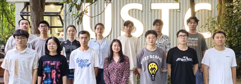
About the University
The University of Science and Technology of China (USTC) in Hefei, Anhui, has been a renowned academic and research institution
since its founding in 1958. It excels in physics, engineering, and computer science, producing influential scientists. USTC’s focus on cutting-edge research attracts global talents and contributes significantly to scientific knowledge.
USTC is among the leading universities in Chinese nanoscience and nanotechnology, with the Hefei National Laboratory for Physical Sciences at the Microscale (HFNL) at the forefront. Equipped with advanced facilities, including Atomic Force Microscopy (AFM), USTC conducts pioneering research in nanomaterials and devices for energy, electronics, and medicine.
NS: Could you share some insights into your current research at the “Integrated Nanoelectronics and X-computing (iNext) lab”? What are the main goals and objectives of your research team?
Shi:
In iNext lab, we focus on exploring the design, integration processes, and device physics of thin-film transistors based on 2D semiconductors and oxide semiconductors, along with their applications in high-performance logic, memory, and brain-inspired computing devices. We anticipate that our research will offer new opportunities for CMOS logic scaling at advanced technology nodes, as well as novel memory architectures and computing paradigms.
NS: In your work, you mention focusing on materials, concepts, and architectures for logic and memory devices. Can you elaborate on some of the novel materials or concepts you find particularly promising for future electronic devices?
Shi:
Yes, I would like to give two-dimensional (2D) semiconductors as an example here for CMOS logic scaling. Abundant-data computing such as big-data analytics, artificial intelligence (AI) and Internet of Things (IoT) demand extreme energy efficiency and concomitant improvement of cost performance of the electronic systems. Silicon-based field-effect transistors (FETs) are the fundamental building blocks of modern computing microprocessors. Following Moore's law, an exponentially increasing number of transistors is integrated into a computing microprocessor, enabled by the scaling of silicon transistors. This makes modern chips faster, more powerful, and cost-effective. Nowadays, the scaling of silicon transistors faces increased technical challenges, such as short-channel effects, making the exploration of alternative new channel materials and device geometries even more crucial for future computing chips.. Atomically thin 2D semiconductors is a new kind of channel materials that could facilitate continued tra sistor scaling, meeting the power, performance, area, cost (PPAC) demands of future electronic devices.
NS: You’ve published numerous research articles in prestigious journals/conferences like Nature Electronics, ACS Nano, and IEDM. Can you highlight a few key findings or breakthroughs from your research that you’re particularly proud of?
Shi:
Yes, I would like to give the key finding in my IEDM paper (2021) as an example. The motivation of this study was the theoretical prediction of ultimate scaling of CMOS logic transistors with atomically thin (monolayer) 2D semiconductors as channel material. However, the uniform monolayer deposition of 2D semiconductors at wafer scale is still challenging. In our IEDM paper (2021), we provided a novel deposition concept for insitu deposition and etching of 2D semiconductors and obtained the uniform monolayer MoS2 film at wafer scale. Furthermore, the scaled transistors with this uniform monolayer MoS2 as channel statistically showed better performance, especially for Vth variation (on par with advanced Si FinFETs) and inhibition to short channel effects, compared to nonuniform monolayer MoS2 based transistors. This work demonstrates the superior electrostatic of atomically thin 2D semiconductors-based transistors and their potential for ultimate transistor scaling.
NS: You’ve had the opportunity to work in both academic and industry research settings. How do these experiences differ, and how have they shaped your approach to nanoscience research?
Shi:
Over my experience in academia and industry, research in academia provides more freedom to pursue the demonstration of new concepts/ideas and a deep understanding of device physics, among other aspects. Meanwhile, the industry, with its industrial infrastructure, can be more beneficial for addressing engineering questions, such as pilot-line process integration, the transition from lab to fab, and industrialization.
NS: Could you tell us more about your work on thin-film transistors (TFTs) and their potential applications in logic, memory, and brain-inspired computing? What role do 2D semiconductors and metal oxides play in your research?
Shi:
In my group, we are exploring thin-film transistors based on two kinds of channel materials: 2D semiconductors and oxide semiconductors. Both of them face similar problems, such as high-quality channel deposition, defect-free modulation, interface engineering, contact resistance, and CMOS integration, among others. The requirements for device performance differ for logic, memory, and brain-inspired computing applications. Typically, logic transistors require scaling capability, high mobility, and inhibition of short-channel effects, among other factors. For memory applications, specifically capacitorless DRAM, one of the main challenges is the trade-off between threshold voltage and on-current for thin-film transistorsbased capacitorless DRAM technology. Devices for braininspired computing are more tolerant of stochasticity, mobility, subthreshold swing, and other factors.
NS: How do you see nanoelectronics and nanotechnology contributing to the development of next generation computing technologies, including quantum computing and neuromorphic computing?
Shi:
Nowadays, digital computing is increasingly capacity-limited and power-limited, which is determined by the slowing down of transistor scaling and the exponential growth of computing needs. This drives most research in nanoelectronics and nanotechnology. Since around 2006, the need for shrinking devices, the bottleneck of the von Neumann computing paradigm, and the limitations of digital information processing have made society realize the urgency of new computing paradigms. One of the promising approaches is to perform computing based on intrinsic nanoelectronics device dynamics, so that each device functionally replaces elaborate digital circuits, leading to adaptive complex computing.