Dynamic Self-Stabilization In The Electronic And Nanomechanical Properties Of An Organic Polymer Semiconductor
- 29 Oct 2023
- Volume 25
- NANOscientific Magazine, Fall-Winter 2023
Illia Dobryden 1,2,8, Vladimir V. Korolkov 3,8, Vincent Lemaur4, Matthew Waldrip 5, Hio-Ieng Un6,Dimitrios Simatos 6, Leszek J. Spalek6, Oana D. Jurchescu 5, Yoann Olivier7, Per M. Claesson1 & Deepak Venkateshvaran 6
1 KTH Royal Institute of Technology, Sweden.
2 Luleå University of Technology, Sweden. 3 Park Systems UK Limited, UK.
4 University of Mons, Belgium. 5 Wake Forest University, NC, USA.
6 University of Cambridge, UK. 7 Université de Namur, Belgium.
8 These authors contributed equally: Illia Dobryden, Vladimir V. Korolkov.
This article has been condensed by NanoScientific under a Creative Commons Attribution 4.0 International License for the purpose of providing shorter and more accessible reading. For the full original article, please go to https://doi.org/10.1038/s41467-022-30801-x - www.nature.com/naturecommunications.
Abstract
The field of organic electronics benefits from new conjugated semi-conducting polymers with resilient molecular backbones and high charge carrier mobilities. Indacenodithiophene-cobenzothiadiazole, previously thought to lack microstructural order, exhibits nanosized domains of high order in its thin films. Its high-performance electrical and thermoelectric properties stabilize rapidly after air exposure, while nanomechanical properties equilibrate over longer timescales due to solvent molecules' gradual release from the surface. This study sheds light on the dynamic evolution and stability of this prototypical organic semiconductor's device properties.
Introduction
Organic semiconducting polymers based on donor-acceptor motifs have gained prominence in organic electronics due to their high charge carrier mobilities, sometimes exceeding 1 cm2/Vs, and their ability to transport both negatively charged electrons and positively charged holes. Among these, a notable subset consists of polymers with a planar backbone as the donor segment, limiting torsion within the molecule. An exemplary polymer demonstrating this sought-after molecular arrangement is indacenodithiophene-co-benzothiadiazole (C16-IDTBT), known for its efficient charge carrier transport along its backbone. In this study, nanoscale regions of high ordering (~15 nm) within device-grade thin films of C16-IDTBT are conclusively shown, enhancing our understanding of its charge transport properties.
Previously investigated through field-effect transistor and Seebeck coefficient measurements, C16-IDTBT displays low torsional disorder and favorable charge transport characteristics. However, this study sheds light on a previously overlooked aspect of C16-IDTBT's behavior. The device characteristics of C16-IDTBT rapidly improve towards ideality during the hours following fabrication and upon exposure to ambient conditions. While efforts have been made to stabilize trap-free hole transport in C16-IDTBT devices using additives, this study demonstrates how self-induced stabilization can occur over time under ambient conditions alone. Additionally, nanomechanical properties of the polymer stabilize with time, displaying texture due to the gradual removal of residual low molecular weight additive solvent molecules from the polymer film.
Understanding the complete electrical, thermoelectric, and nanomechanical properties of C16-IDTBT, as well as their time evolution, is crucial for its application in next-generation air-stable polymer semiconductor-based electromechanical devices. This research highlights the significance of strictly connecting measured properties to ambient conditions under which they are reported as organic materials often exhibit dynamic evolution. It also emphasizes the importance of reporting all fabrication and characterization procedures to ensure better reproducibility between different labs, advancing the field of organic electronics.
Results and discussion
This research utilizing high-resolution transmission electron microscopy (TEM) has presented compelling evidence of nanoscale order within C16-IDTBT thin films, contradicting previous assumptions about their largely amorphous microstructure. Preserving the pristine large-area structural integrity of these thin films, the atomic force microscopy (AFM) was employed to observe minute regions with aligned polymer filaments, unveiling a nanoscale periodicity of 1.6 nm. The nanoscale order confirmed earlier findings from high-resolution TEM and scanning tunneling microscopy (STM), highlighting a liquid crystalline-like character with aligned polymer backbones. This study serves as an essential demonstration that simple sample preparation techniques can facilitate the observation of nanoscale ordering in C16-IDTBT thin films.

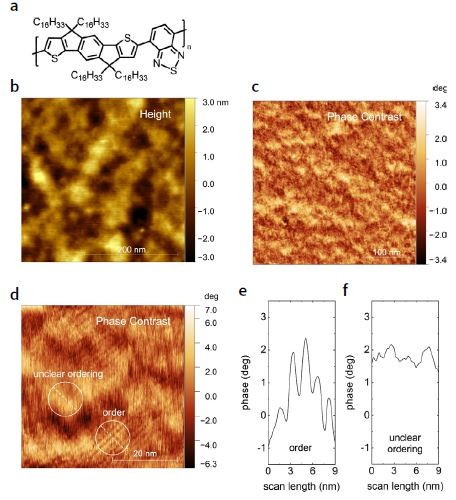
Figure 1(a) shows the chemical structure of C16-IDTBT, a copolymer of indacenodithiophene (IDT) and benzothiadiazole (BT) units. Figures 1(b) and (c) display height topography and phase contrast images obtained with an atomic force microscope (AFM) on a stabilized thin film of C16-IDTBT. Aligned polymer filaments are observed at this resolution. A high-resolution image (Fig. 1(d)) shows two regions within 30 nm of each other; one with significant order and the other with unclear ordering. The high-order region exhibits bright streaks corresponding to individual polymer backbones. The thin film's molecular backbone faces down on the substrate, with π-π stacking perpendicular to the substrate. AFM scans reveal a periodicity of 1.6 nm in the ordered region (Fig. 1(e)). This periodicity does not confirm STM findings of sidechain interdigitation in dispersed C16-IDTBT molecules. However, it aligns with recent TEM investigations, showing a liquid crystalline-like character without interdigitation of alkyl side chains in the film. Polymer backbones are parallel with their molecular faces looking up, and the bright regions are attributed to non-planar sp3 bridging carbons in the IDT units (Fig. 1(f)). These AFM results confirm the observed length scale of order and the parallel polymer backbone arrangement seen in high-resolution TEM and STM studies. Notably, the 50 nm thick films were spin-coated with common parameters used for C16-IDTBT-based organic transistors, requiring simple sample preparation.
A study was conducted to investigate how the electrical and thermoelectric properties of C16-IDTBT-based devices evolve over time. This organic semiconductor is known for its high charge carrier mobilities. Both organic thin-film transistor characteristics and the gate voltage modulated Seebeck coefficient were measured within the same device during the study. The results showed a remarkable improvement in the electrical behavior of the device when exposed to ambient air. The on-current increased significantly, and the subthreshold swing reduced to a remarkably low value, indicating improved charge transport efficiency. After a month of air exposure, the device exhibited textbook-like output characteristics, while devices stored in a nitrogen glovebox continued to display non-ideal behavior. This enhancement was attributed to a p-doping/electron-trapping mechanism involving oxygen, which increased the hole carrier concentration and improved charge extraction and injection.
The study also investigated the Seebeck coefficient as a measure of entropy per unit charge in the device and its relation to ambient air exposure. The reduction of the Seebeck coefficient over time suggested an increasing number of carriers participating in energy and entropy transport. Initially, the device contained more carriers in trap states that did not contribute to entropy transport at low carrier accumulation. The most rapid changes in the Seebeck coefficient occurred within the first 24 hours of air exposure, followed by gradual changes. The researchers speculated that a structural reorganization within the film, caused by the release of residual solvent over time, might accompany this behavior. These findings provide insights into the dynamic evolution of C16- IDTBT-based devices and emphasize the importance of ambient conditions in determining their electrical and thermoelectric properties.
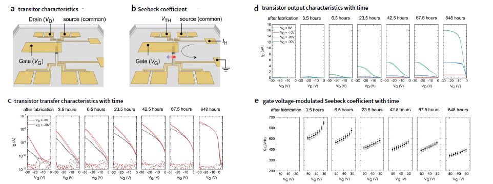
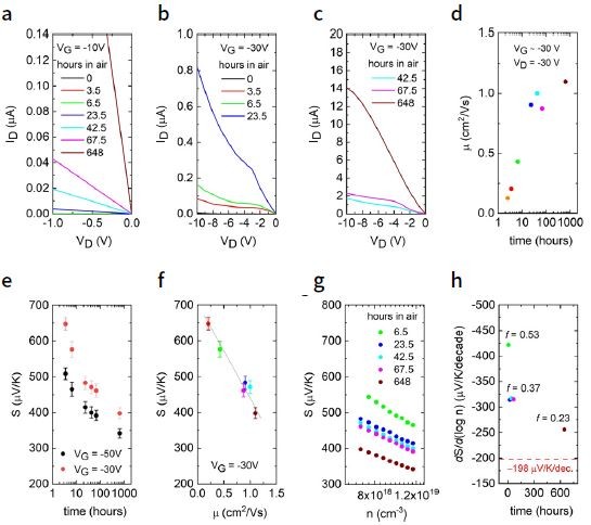
Figure 2 and Figure 3 depict the temporal evolution of electrical and thermoelectric properties in C16-IDTBT based devices. In the case of Figure 2, measurements using organic thinfilm transistors and gate voltage modulation revealed rapid enhancement of the device's electrical characteristics within the initial hours of air exposure, accompanied by significant changes in the Seebeck coefficient. This improvement is attributed to ambient air and is believed to involve a p-doping/ electron-trapping mechanism mediated by oxygen. Similarly, Figure 3 illustrates that upon exposure to ambient air, C16- IDTBT devices exhibited swift enhancements, indicating reduced contact resistance and improved carrier injection and extraction. Over time, non-idealities in transistor output characteristics disappeared, possibly due to induced carriers filling traps and enhancing charge transport. The Seebeck coefficient exhibited two linear regimes, initially reducing rapidly and then gradually over time, while hole mobility initially increased and later stabilized. Notably, the relationship between the Seebeck coefficient and saturation mobility appeared linear, with both transport coefficients showing an exponential dependence on time.
The study also examined the nanomechanical properties of C16-IDTBT thin films. Unlike electrical properties, the nanomechanical properties did not change significantly with ambient exposure but stabilized over time. Regarding its nanomechanical properties, there is no difference between the evolution of organic films stored in ambient air and organic films stored in a nitrogen glovebox. Also, in contrast to C16-IDTBT’s electronic property evolution, the polymer’s nanomechanical properties stabilize on a longer time scale owing to a mechanism pinned not to oxygen diffusion, but to a gradual sweating-out of residual, low molecular weight solvent molecules from the organic polymer film’s surface.
Overall, the research highlights the dynamic nature of C16- IDTBT-based devices and the crucial role of ambient conditions in shaping their electrical, thermoelectric, and nanomechanical properties. The study sheds light on the complex interactions within the devices, providing valuable insights for the development of advanced polymer semiconductor-based electromechanical devices.
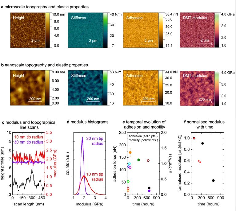
(c) Line scan of the modulus and topography along the dotted white lines shown in (b) measured using a tip radius of 10 nm. A scan of the modulus with a tip radius of 30 nm is shown in purple for comparison63. (d) Comparison of modulus histograms measured with two different tip radii; a 30 nm tip radius (larger than ordered film features) and a 10 nm tip radius (equivalent or less than ordered film features). (e) Comparison showing how the film adhesion changes far slower with time than the saturation mobility. (f) Normalized modulus measured on different C16-IDTBT samples using two different AFMs. The black dots correspond to the measurements on a Park Systems NX20 and the red dots correspond to measurements on a JPK NanoWizard 3 Atomic Force Microscope. The modulus reduction and homogenization that accompanies the reduction in adhesion force takes place on a time scale longer than the stabilization of the saturation mobility.
In addition, the study investigated the temporal evolution of electrical, thermoelectric, and nanomechanical properties in C16-IDTBT thin films. The nanomechanical properties were probed using AFM to map surface topography, stiffness, adhesion, and modulus. Films exposed to ambient conditions showed improved electrical characteristics and carrier mobility over time. The Seebeck coefficient and saturation mobility demonstrated a linear relationship, indicating a new scaling law. The improvement in device characteristics was attributed to oxygen diffusion, doping, and microstructure rearrangement due to solvent removal. The nanoscale mechanical modulus exhibited texture, with nanocrystalline regions being stiffer than amorphous regions.
Furthermore, the study revealed that the nanomechanical properties of C16-IDTBT films continued to change over several weeks, with a gradual reduction in adhesion force and modulus due to solvent sweating out. This process occurred over a longer timescale than the stabilization of electronic mobility. The results underscored the importance of carefully documenting the conditions under which multifunctional properties of organic polymer devices are reported.
In summary, the research shed light on the intricate temporal dynamics of C16-IDTBT thin films, providing valuable insights into their electrical, thermoelectric, and nanomechanical behaviors. The findings contribute to the understanding of organic semiconductors and highlight the significance of environmental factors in shaping their performance characteristics.
Figure 4(a) and (b) display the nanomechanical properties of a C16-IDTBT thin film, stored in ambient conditions for several weeks to facilitate the evaporation of residual solvent molecules. Park System’s PinPoint Nanomechanical measurement mode on an NX20 AFM was employed to examine the microscale topography, stiffness, adhesion, and elastic modulus. This method extracts nanomechanical properties using force curves that map tip-sample interactions. The film exhibited an average modulus around 2 GPa with homogeneity over a 5 μm x 5 μm area. Figure 4(b) portrays nanoscale properties, showing significant texture in stiffness, adhesion, and modulus over a few hundred square nanometers. The relationship between the ordered and disordered regions was analyzed in Fig. 4(c) through line scans of topography and modulus, where texture in modulus was not influenced by tip artifact. With a 10 nm tip radius, notable features were observed on a 50 nm or smaller scale, suggesting crystallinity differences between ordered and disordered regions. However, the 30 nm tip radius produced uniform modulus readings. Figure 4(d) demonstrated histogram asymmetry, indicating potential crystallinity differences.
In contrast, a C16-IDTBT film without extended stabilization showed distinct nanomechanical properties. Over time, adhesion force and elastic modulus decreased. Initial adhesion force was high three days after film fabrication. While electronic properties stabilized within three days, adhesion gradually changed over weeks due to solvent outgassing. After a month, adhesion reached ~27 nN, consistent with stabilized thin films and correlated with other nanomechanical measurements. Figure 4(f) illustrated a significant reduction in average modulus (E(t)/E(72)) over time due to solvent evaporation, a process slower than hole mobility reaching its threshold value. Dynamic bubble formation was also observed on the film surface.
Methods
Fabrication of transistor and Seebeck devices and its measurement sequence
Fabricating devices: Gold electrodes micropatterned using optical lithography and thermal evaporation. A resistive stripe heater is added. Organic semiconductor C16-IDTBT overlaps the electrodes, avoiding cross talk. Organic layer 200 microns long, 1 mm wide. Source and drain electrodes double as on-chip thermometers. 500 nm Cytop-M dielectric layer processed over organic semiconductor and substrate. 25 nm gold gate electrode deposited over the dielectric, covering the organic semiconductor. Transistor characteristics and Seebeck coefficient measured with gate voltage in monitored time sequence (see Supplementary Info Section 4 in the original paper). Steps carefully executed to limit air exposure. Device measured under vacuum. Seebeck measured again after ambient exposure. Detailed procedures in Supplementary Information.
Pinpoint nanomechanical measurements and AFM based phase topography
Park Systems NX20 Atomic Force Microscope (Park Systems Co., Suwon, Korea) was used for both topography and nanomechanical properties measurements conducted in ambient conditions at 22°C using PinPoint nanomechanical measurements and AFM phase topography techniques. Highresolution phase maps were obtained using a novel higher eigenmode approach with Multi75Al-G cantilevers excited at the 3rd eigenmode [V. V. Korolkov et al., Nat. Commun. 10, 1537 (2019)]. Nanomechanical data was collected with PinPoint Nanomechanical mode [S. Kim et al., Nanomaterials 11(6), 1593 (2021)] on the same instrument, enabling simultaneous acquisition of topographical maps and force-distance curves at each pixel. Automated analysis provided nanomechanical properties like modulus, adhesion, deformation, stiffness, and energy dissipation. AC160TS cantilevers (Olympus, Japan) with a nominal spring constant of 42 N/m were used, calibrated before measurements. The C16-IDTBT thin film sample investigated was "stabilized," allowing solvent molecules to sweat out from its surface for reliable measurements after a few weeks.
Data availability
The data used in this study are presented in the text and the Supplementary Information (https://www.nature.com/articles/ s41467-022-30801-x#MOESM1). Additional data are available from the corresponding authors upon reasonable request. The Atomic Force Microscopy and Nanomechanics dataset used in Fig. 1 and Fig. 4, are available at Cambridge University’s online repository: https://doi.org/10.17863/CAM.84546.