Beyond Potential: A New Frontier In Surface Charge Quantification With FEM/KPFM-Hybrid Approach
- 19 Aug 2025
- Volume 28
- NANOscientific Magazine, 2025
Felix Pertl, Soft & Electrified Materials Lab, Institute of Science and Technology Austria (ISTA), Klosterneuburg, Austria
Adapted from Presentation, Edited by NanoScientific
From Balloons to Breakthroughs in Charge Mapping
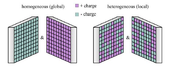
Rubbing a balloon on your hair and watching it stick to a wall might seem like a simple childhood experiment, but for PhD student Felix Pertl from ISTA, it highlights a major unsolved problem in surface science. This effect, known as contact electrification (CE), is the transfer of charge when two neutral materials touch. Despite being widely observed, its mechanisms remain unclear [1-2]. Key questions—such as which charge carriers are involved, what drives the transfer, and whether the resulting charge distribution is homogeneous or heterogeneous—are still unanswered. Possible explanations include transfer of electrons or ions via induced dipoles, adsorbed water layers, flexoelectric effects, or combinations thereof, with implications spanning electronics, lightning formation, and biology.
To study CE at the nanoscale, researchers use Kelvin Probe Force Microscopy
(KPFM). Pertl employs KPFM to examine whether surface charge is homogeneously or heterogeneously distributed (Figure 1) [3-4]. However, while KPFM measures voltage related to surface charge, converting this to true charge density remains a challenge.
At the NanoScientific Forum Europe 2024, Pertl presented a refined approach combining KPFM with Finite Element Method (FEM) simulations to overcome this issue, enabling rigorous extraction of true surface charge densities [5].
The Limits of Traditional KPFM
KPFM has long served as a stable technique in nanoscale characterization,
capable of mapping the surface potential between a conductive atomic force microscope (AFM) tip and a sample. By applying an AC/DC voltage and measuring the resulting electrostatic force, KPFM determines variations in work function or surface potential at nanometer resolution.
However, Pertl emphasized a critical shortcoming of the conventional approach: “Everyone always shows the potential,” he said, “but I care more about the charge.” In other words, surface potential data—while useful—is only an indirect representation of the true quantity of interest: the charge distribution on the sample’s surface.
The most common workaround is the simplistic parallel-plate capacitor model, which assumes the AFM tip and the sample form a basic capacitor. The problem? This approach grossly underestimates charge density because it ignores the complex geometry and electrostatic interactions inherent in the real-world tip–sample system (Fig. 2).
Toward a Physics-Accurate Charge Mapping
To address these limitations, Pertl proposes a more rigorous physical model based on energy equations and finite element simulations. His process begins with acknowledging the electrostatic energy of the system when a single point charge q is on the surface
Welec = u0 q2 + u1 qV + u2 V2
where the u0, u1, u2 are geometric parameters and V is the potential between tip and back electrode. The first term, u0q2, comes from the charge interaction with its images in the cantilever/insulator/ground capacitor.
The second term comes from the charge’s interaction with the capacitor field. The last term is the energy of the capacitor itself. KPFM uses a voltage V = Vbg - VDC + VAC sin(ωt), where Vbg is any background potential difference in the absence of charge added from contact (e.g. related to the contact potential differences or vertically separated bulk charges) and VAC/DC are AC/DC driving voltages. Taking the negative derivative of the electrostatic energy with respect to the tip deflection, z, gives the vertical force which can be separated into a DC component, a component at ω and a component at 2ω. Denoting z-derivatives as primed, the ω component is
Fω= -u'1qVAC sin(ωt) - 2u'2 (Vbg - VDC) VAC sin(ωt)
In AM-KPFM, a potential VDC is applied to nullifiy the force at frequency
ω and solving for VAM = VDC, we have
VAM= 1/2 (u'1 q)/(u'2) + Vbg
Thus, the presence of a point charge modifies the KPFM voltage of a
neutral insulator surface by the addtion of the term 1/2 u'1 q/u'2.
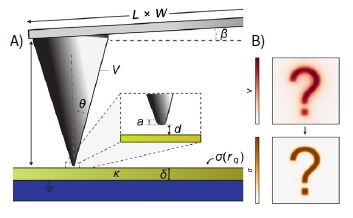
insulator with varying surface charge density σ
is complex and depends on many parameters. B) In
KPFM, one measures a potential map, V that is caused
by the surface charge, but in a highly non-trivial way.
Enter Green’s Functions and FEM Simulations
For realistic samples, which host continuous charge distributions rather
than isolated point charges, u'1 and u'2 can be related to a Green’s function—
a mathematical construct describing the response of a system to a unit input (in this case, a unit surface charge). The convolution between surface potential V and a continuous charge density σ can then be written as:
V(rt )= ∫∫ G(|rt - rq |)σ(rq )dxq dyq
Obtaining an analytical expression of the Green’s function for this complex
geometry is almost impossible. To circumvent this, Pertl uses finite element simulations to numerically construct the Green’s function for the exact setup used in experiments (Fig. 3).
By systematically placing point charges beneath the tip and simulating the electrostatic response across the entire scan area, a full 3D map of the Green’s function is built. From here, the charge density can be extracted via deconvolution using Fourier transform techniques.
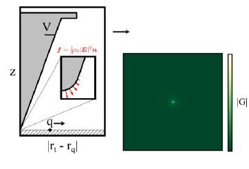
a radially symmetric 2D map
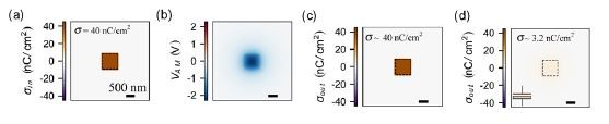
Synthetic Validation and Experimental Confirmation
Before applying the method to real data, Pertl validated it on synthetic samples with known charge distributions. A square patch with defined charge density was processed through the simulation pipeline, producing a potential map showing expected convolution effects, such as blurring and fringe fields. The inverse transformation accurately recovered the original charge density within a small margin of error (Fig. 4), confirming the method’s validity.
In the lab, Pertl tested this on a clean silicon oxide surface. By bringing the AFM tip into contact and slightly scratching it, he introduced localized surface charges. The resulting KPFM map showed a diffuse patch similar to the synthetic result (Fig. 5).
Using FEM simulations based on precise setup parameters—tip geometry, material properties, and tip-sample distance—he generated the Green’s function. Deconvolution of the potential data then yielded a charge density map with values matching the synthetic input (~40 nC/cm²). This demonstrated quantitative accuracy and revealed fine spatial details invisible from potential data alone.
recovered charge so small it is barely visible. Additionally, sharp spatial features of original charge distribution are lost.
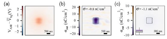
Advantages Over the Capacitor Model
Pertl revisited the conventional capacitor model for comparison. When the same potential data was processed using the simplified model, the resulting charge density was underestimated by more than a factor of ten. This stark discrepancy underscores the importance of geometry-aware modeling, especially for high-resolution, quantitative analysis.
What makes Pertl’s method transformative is its ability to move from qualitative imaging to quantitative metrology. It enables researchers to measure actual surface charge density at the nanoscale—turning KPFM from a relative mapping tool into an absolute characterization technique.
Implications and Future Applications
Pertl’s approach paves the way for more precise studies of contact electrification, dielectric breakdown, charge trapping, and material aging. It
holds particular promise for fields such as:
• Flexible electronics, where contact-induced charging can affect performance.
• Energy storage, where charge leakage or accumulation alters behavior over time.
• Triboelectric devices, where contact-induced charges are harnessed for energy harvesting.
• Nanoionics and memristive devices, which rely on ionic and charge transport mechanisms.
Moreover, his method could potentially be adapted for in-situ or operando
experiments where the dynamics of charge movement and accumulation
are tracked in real-time under electrical bias or mechanical stress.
Conclusion: A New Era for Surface Charge Microscopy
Felix Pertl’s contribution is more than a technical enhancement—it represents
a conceptual shift in how we analyze and understand surface charge phenomena. By integrating high-fidelity simulations with established KPFM techniques, he has opened new avenues for quantitative, spatially resolved charge mapping.
In doing so, Pertl offers a tool that could redefine how scientists study everything from friction and wear to semiconductor performance and sensor sensitivity. As the quest to understand contact electrification continues, his work stands as a crucial step toward unraveling the mysteries of surface charge behavior—one Green’s function at a time.
References
1. D.J. Lacks and R.M. Sankaran. Contact electrification of insulating materials, Journal of Physics D: Applied Physics 44, 453001 (2011).
2. T. Shinbrot and DJ Lacks. Long-standing and unresolved issues in triboelectric charging, Nature Reviews Chemistry 3, 465 – 476 (2019).
3. H.T. Baytekin, A.Z. Patashinski, M. Branicki, B. Baytekin, S. Soh and B.A. Grzybowski. The Mosaic of Surface Charge in Contact Electrification, Science 333, 308 (2011).
4. Shinbrot, T., Komatsu, T. S., & Zhao, Q. (2008). Spontaneous tribocharging of similar materials. Europhysics Letters, 83(2), 24004.
5. Pertl, F., Sobarzo, J. C., Shafeek, L., Cramer, T., & Waitukaitis, S. (2022). Quantifying nanoscale charge density features of contact-charged surfaces with an FEM/KPFMhybrid approach. Physical Review Materials, 6(12), 125605.

The Waitukaitis group: Felix Pertl, 3rd from left
Felix Pertl is a PhD student in the Waitukaitis group, studying charge transfer aftercontact electrification using Kelvin Probe Force Microscopy. He began this work as an intern in 2021 after completing his master’s in Technical Physics at the Technical University of Graz, where his thesis with Lam Research focused on defects on silicon wafers. He earned his bachelor’s in physics there in 2019. Originally from Klagenfurt, Austria, Felix enjoys padel tennis, hiking, and skiing.