Inside The Atomically Thin Frontier: How Spm Is Advancing 2d Tmd Characterization And Device Integration
- 20 Aug 2025
- Volume 28
- NANOscientific Magazine, 2025
At the 2024 NanoScientific Symposium Americas, Dr. Albert Minj of imec presented a masterclass in precision metrology at the nanoscale. His talk offered a rare and revealing glimpse into the challenges and opportunities at the intersection of advanced scanning probe microscopy (SPM) and two-dimensional (2D) semiconductors—particularly transition metal dichalcogenides (TMDs), such as molybdenum disulfide (MoS₂) and tungsten disulfide (WS₂).
Imec, headquartered in Belgium, is a world-leading R&D hub known for its work in logic, memory, photonics, and energy. As part of imec’s metrology department, Minj operates at the center of this ecosystem, helping drive breakthroughs in characterization tools critical for the semiconductor industry’s transition to atomically engineered devices.
Monolayers, Mobility, and the Materials Challenge
The semiconductor industry is reaching physical and practical limits with traditional silicon-based scaling. Enter 2D materials. These atomically thin layers—just a few atoms thick—offer tantalizing potential for continued device miniaturization with improved electrostatics, scalability, and performance.
To make these materials viable for logic applications, however, imec is targeting the growth of high-quality, single-crystal monolayers across full wafer scales—up to 200 mm and beyond. Both n-type and p-type conduction must be achieved with high mobility. But the success of these efforts depends not just on growth processes, but also on the precision of the tools used to measure them.
Environment Matters: A Case Study in Vacuum vs. Air
A compelling early example Minj shared was the behavior of monolayer MoS₂ exposed to ambient conditions. Using four-point probe measurements on a sample grown on sapphire, imec researchers observed a dramatic increase in resistance—doubling within just 30 minutes of air exposure.
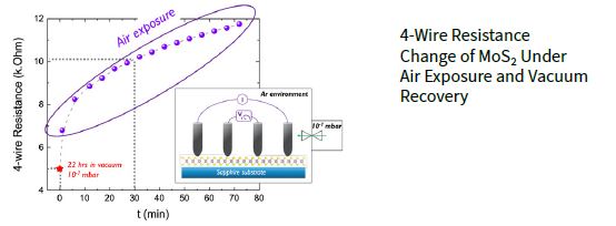
This degradation is caused by interaction with environmental elements such as oxygen, water vapor, and airborne contaminants, which interfere with the material's electrical properties. Significantly, this effect was reversible. After prolonged exposure to high vacuum, the initial conductivity was largely restored.
Such results highlight the inadequacy of ambient characterization for truly understanding 2D materials. They also motivated the team to turn to high-vacuum conductive atomic force microscopy (C-AFM) using Park Systems instrumentation to delve deeper.
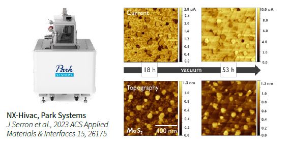
Conductive AFM: Revealing the Surface Transformation
C-AFM current maps of monolayer MoS₂ showed dramatic changes Over time during prolonged scanning under vacuum. Initially, the maps revealed distinct inhomogeneities—patches of low conductivity and small features that suggested structural discontinuities or contamination. However, after more than 50 hours of continuous scanning, the current maps homogenized, and many of the patches vanished.

The conclusion? The AFM tip, in vacuum, had physically displaced or removed intercalated water molecules and contaminants trapped between the 2D layer and its substrate. This finding was corroborated by STM (scanning tunneling microscopy) data, which visually captured intercalated water pockets and showed their disappearance over time. This result opens the door to a potentially transformative approach: correlating intercalation signatures with underlying defectivity—a path toward rapid screening of TMD quality.
Kelvin Probe Force Microscopy: Layer-Dependent Potential
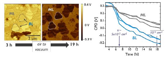
To further analyze these transformations, Minj's team turned to Kelvin Probe Force Microscopy (KPFM), which maps the surface potential with nanometer precision. In 2D materials, the contact potential difference (CPD) measured by KPFM is not simply a function of the material’s work function. Rather, it is heavily influenced by interface charges, environmental factors, and the number of layers.
Initial CPD maps showed that bilayer regions exhibited different potentials compared to the monolayer background. However, after prolonged vacuum exposure, this contrast reversed—an indication that charge distributions had changed. Applying theoretical models, the team estimated changes in carrier concentration, observing an increase from approximately 5 × 10¹² to 1 × 10¹³ cm⁻².
Yet, even in deep accumulation conditions, some areas—especially grain boundaries and bilayer island edges—showed persistent difficulty in screening charges.
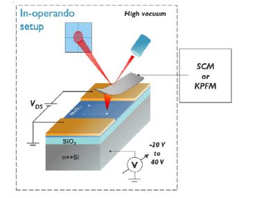
From Passive Mapping to Active Devices: In Operando SPM
Beyond passive characterization, Minj emphasized the power of in-operando SPM—probing a device while it is functioning. Using a standard FET structure with a monolayer MoS₂ channel, nickel source–drain contacts, and a back-gated silicon substrate, the team used KPFM to monitor CPD profiles along the channel under varying gate voltages.
The maps showed band bending and potential shifts consistent with carrier injection and depletion. This extended to the contact edge—where the metal-semiconductor junction often limits device performance—allowing the team to observe how the interface responded to gate bias in real time.
By comparing the results to simulations, the team found that agreement broke down in some ranges—likely due to interface traps. Further, CPD delta analysis helped quantify local band bending behaviors.
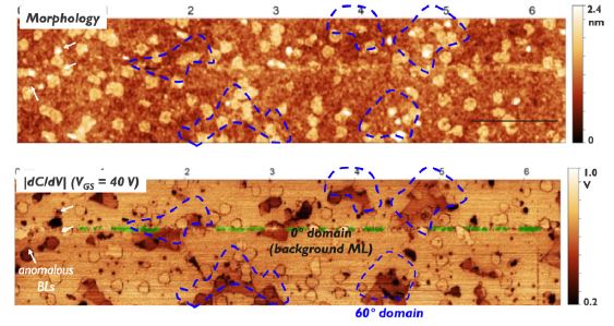
Grain Boundaries and Orientation Effects
One of the most illuminating applications of in-operando KPFM was the visualization of grain boundaries. Minj’s team classified segments based on their alignment to current flow. Those perpendicular to current flow direction created carrier accumulation zones and acted as potential barriers, while parallel segments showed little impact.
Scanning capacitance microscopy (SCM) further complemented these insights. Differential capacitance measurements showed that misoriented grains and certain bilayer domains harbored higher electrically active defect densities, as reflected in suppressed capacitance signals.
A Minj et al., 2024 ACS nano 18, 10653
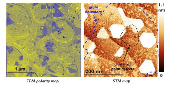
Corroboration with TEM and STM
TEM analysis revealed that 60°-rotated domains—clearly mapped through polarity contrast—harbored point defect clusters, as confirmed by STM imaging. These findings validated SCM and KPFM measurements, showing that electrical behavior tracked closely with crystallographic and chemical non-uniformities.
Looking Ahead: Metrology Perspectives
Minj concluded by outlining key strategic directions for the field:
• Standardization of characterization methods is imperative to eliminate variability across labs and instruments. The 2D materials community urgently needs consensus on environmental control, measurement parameters, and interpretation models.
• Integration of metrology tools with probe stations will enable high-throughput, in-operando device measurements—transforming how labs screen new materials and optimize fabrication.
• Fast, quantitative defect analysis using tools like STM, c-AFM, friction mapping, and others should become routine to identify local disruptions at the atomic scale.
Conclusion
Dr. Albert Minj’s work exemplifies the evolving role of scanning probe microscopy—not merely as an imaging technique, but as a quantitative platform that drives materials science forward. From water intercalation and defect mapping to in-operando device diagnostics, scanning probe microscopy is rapidly becoming the keystone technology for developing next-generation 2D semiconductors.
As the semiconductor industry marches into the atomic era, the future of logic devices may well hinge on what SPM reveals—one defect, one grain boundary, one layer at a time.

Dr. Minj has worked with Scanning Probe Microscopy (SPM) since 2009. He
earned his PhD from the University of Bologna and completed postdoctoral
research at CNRS in France, where he studied crystallographic defects in
wurtzite crystals using Transmission Electron Microscopy and developed surface
photovoltage KPFM for defect analysis in ultra-wide bandgap materials. In 2018,
he joined imec in Belgium—the birthplace of Scanning Spreading Resistance
Microscopy (SSRM)—where he is currently a researcher.
From 2020 to 2022, he led a Marie Curie Fellowship advancing SPM techniques
for doping and defect analysis in GaN power devices and 2D materials. His
ongoing research focuses on 2D systems, carbon nanotubes, and new AFM
modes. He works within imec’s 12-member SPM team, led by Dr. Thomas
Hantschel, which supports both scientific innovation and metrology across
imec’s research programs.
Minj at Graphene week, Gothenberg, Sweden 2023.