Mapping Ions And Polarons With Photoinduced Force Microscopy: Unlocking The Inner Workings Of Organic Mixed Conductors
- 19 Aug 2025
- Volume 28
- NANOscientific Magazine, 2025
Prof. Connor Bischak, Department of Chemistry, University of Utah
Adapted from Presentation, Edited by NanoScientific
Organic mixed ionic-electronic conductors (OMIECs) are ushering in a new paradigm in the field of soft electronics. Distinguished by their ability to transport both electronic and ionic charges, OMIECs offer an unprecedented platform for interfacing electronic devices with dynamic environments such as biological systems. In a recent lecture delivered at the 2024 NanoScientific Symposium Americas, Prof. Connor Bischak presented his group’s latest advances in visualizing charge dynamics in these complex systems using Photoinduced Force Microscopy (PiFM).
Mixed Conduction and Its Challenges
Unlike traditional inorganic semiconductors like silicon, which are purely electronic conductors, OMIECs combine the conductive properties of conjugated polymers with side chains that facilitate ionic transport. This dual transport mechanism enables volumetric electrochemical doping, in which ions from an adjacent electrolyte penetrate the bulk of the polymer to compensate for injected electronic carriers. This is in stark contrast to the surface-confined charge accumulation in conventional materials, which is limited by electric double layer formation.
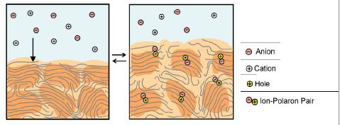
Prof. Bischak introduced the core concepts behind these materials, focusing on conjugated polymers functionalized with ethylene glycol-type side chains. These side chains allow the ingress of ions—typically from aqueous electrolytes—into the polymer backbone under applied bias, forming polaron-ion pairs. These pairs represent the basic charge storage and transport units in OMIEC-based devices such as organic electrochemical transistors (OECTs) and bioelectronic interfaces. However, a major challenge in the development and optimization of these materials is the lack of spatially resolved techniques that can directly visualize where ions and polarons accumulate during operation. Without such information, the design of more efficient devices remains largely empirical.
PiFM: A Window into Nanoscale Charge Distribution
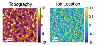
To address this gap, Prof. Bischak’s group with graduate student Seth Jackson has employed Photoinduced Force Microscopy (PiFM)—a hybrid scanning probe technique that combines the spatial resolution of atomic force microscopy (AFM) with the chemical sensitivity of infrared spectroscopy. PiFM detects the photoinduced forces between the AFM tip and the sample, enabling the mapping of specific vibrational modes associated with distinct chemical species such as ions in a polymer matrix.
Through PiFM, the team achieved nanoscale chemical imaging of ion and polaron distributions in polymer thin films under electrochemical bias. This method allowed them to observe how different regions of the film respond heterogeneously to doping, revealing dynamic rearrangements during charge injection and extraction.
For instance, they identified domains within the polymer where ions preferentially accumulated, forming more heavily doped (polaron-rich) regions, while other areas remained relatively undoped. These spatial heterogeneities are likely rooted in the semicrystalline morphology of OMIECs, where crystalline domains offer different levels of ionic accessibility compared to amorphous regions.
Such insights are crucial, as they help explain the observed electrical behavior of devices and guide the synthesis of polymers with more uniform or controllable doping profiles. The ability to directly image the formation and distribution of polaron-ion pairs at the nanoscale represents a significant advance in the field.
Beyond Microscopy: Integrated Materials Discovery
While PiFM has become a central tool in the Bischak Lab’s arsenal, the group also adopts a broader strategy for materials development. Their research is supported by robotic synthesis platforms inspired by arcade-style claw machines, capable of performing automated deposition and characterization of polymer films. This setup enables rapid screening of candidate materials under reproducible conditions, with integrated photoluminescence and absorption spectroscopy for immediate feedback.
These automation tools allow the lab to systematically explore the effects of processing variables—such as solvent choice, coating speed, and electrolyte composition—on film morphology and electrochemical response. The data generated can be coupled with PiFM insights to construct comprehensive structure–function relationships.
In addition, Prof. Bischak’s team investigates phase transitions in 2D hybrid perovskites and other soft materials, using time-resolved optical spectroscopy to track melting transitions and dynamic structural rearrangements. This work complements their study of OMIECs by expanding their understanding of ion–lattice interactions and charge transport in mixed conduction systems.
Toward Better Bioelectronic Devices
One of the key application targets for OMIECs is in bioelectronics, where materials must interface effectively with the ionic environments of cells and tissues. The volumetric capacitance enabled by OMIECs allows
Them to transduce weak biological signals with high fidelity and low impedance, making them ideal for neural interfaces, biosensors, and drug delivery systems. By uncovering the spatial dynamics of electrochemical doping, Prof. Bischak’s work provides foundational knowledge to optimize these interfaces. More homogeneous ion and polaron distributions could lead to more stable device operation, faster switching times, and improved biocompatibility.
Conclusion and Future Directions
Prof. Connor Bischak’s work represents a fusion of advanced characterization, synthetic chemistry, and device engineering, all aimed at solving one of the central challenges in soft electronics: understanding and controlling mixed conduction at the nanoscale. By leveraging the unique capabilities of Photoinduced Force Microscopy (PiFM), his group has demonstrated the ability to map the location of ions and polarons within conjugated polymer thin films with high spatial precision.
Their findings indicate that ions tend to preferentially localize within crystalline regions of the polymer—a critical insight that may influence how these materials are processed and engineered for device performance. The group has also proposed a promising strategy to improve n-type OMIECs by blending polymers with complementary electronic and ionic transport properties, potentially overcoming historical challenges in n-type material design.
Looking ahead, the Bischak Lab is exploring how to extend PiFM into solid–liquid interfaces, which would enable real-time probing of electrochemical processes in environments that more closely mimic operating devices or biological conditions. As the field moves toward increasingly complex and integrated devices, the ability to “see” where charges go—and how they interact with the surrounding medium—will be essential. PiFM is proving to be not just a tool of analysis, but a guidepost for the rational design of the next generation of responsive, bio-integrated, and high-performance soft electronics.
What Is PiFM?
Photoinduced Force Microscopy (PiFM) is a hybrid analytical technique that combines elements of Atomic Force Microscopy (AFM) and infrared (IR) spectroscopy to achieve label-free, non-destructive chemical imaging at the nanoscale. While AFM excels at imaging topography by detecting minute forces between a sharp tip and the sample surface, it traditionally lacks chemical specificity. IR spectroscopy, on the other hand, identifies molecular vibrations specific to chemical bonds but suffers from diffraction-limited spatial resolution (typically >1 μm). PiFM cleverly integrates the two.
How Does PiFM Work?
At the heart of PiFM is the detection of photo-induced forces between an AFM tip and the sample surface under infrared illumination:
-
Excitation: A tunable IR laser illuminates the sample. If the frequency of the IR light matches a vibrational mode of a chemical group in the sample, it absorbs the light, leading to localized photothermal expansion or a change in dipole moment.
-
Force Generation: These light-induced phenomena generate a localized attractive force between the tip and sample, which oscillates at characteristic frequencies.
-
Force Detection: The AFM cantilever senses these oscillating forces. By demodulating the response at specific harmonics of the cantilever’s resonant frequency, PiFM distinguishes the photo-induced force from background noise.
-
Spectroscopy and Imaging: By scanning across the surface and tuning the laser, PiFM maps out both the topography and chemical composition of the sample with nanometer resolution—often better than 10 nm.
Why Is PiFM Unique?
PiFM stands out because it offers:
• Simultaneous topographic and chemical imaging
• Sub-10 nm spatial resolution in chemical maps
• Non-contact, non-destructive analysis
• Label-free identification of functional groups and material phases
• Sensitivity to local dielectric, optical, and vibrational properties
This makes it ideal for investigating heterogeneous, soft, or nanostructured materials—including polymers, biological tissues, 2D materials, and hybrid devices.
Applications of PiFM
PiFM has been successfully applied in diverse scientific and technological domains:
• Polymer and composite materials: Mapping domain compositions, phase separation, and chain orientation
• 2D materials and semiconductors: Probing heterostructures, grain boundaries, and local doping
• Energy materials: Investigating degradation and ion migration in batteries and fuel cells
• Biomaterials and tissues: Identifying proteins, lipids, and other macromolecules in situ
• Organic electronics: Studying morphology and doping dynamics in organic solar cells and transistors
Watch how PiFM works on YouTube:
https://www.youtube.com/watch?v=by3tNOCWw1w
Dr. Bischak is an Assistant Professor of Chemistry at the University of Utah (appointed 2021). He earned a B.S. in Chemistry from Haverford College (2010), completed a Fulbright Fellowship at Ruhr University Bochum (2010-11), and received his PhD in Chemistry from UC Berkeley in 2017 under Prof. Naomi Ginsberg. He then served as a Washington Research Foundation and Cottrell Postdoctoral Fellow with Prof. David Ginger at the University of Washington (2018-21), focusing on organic mixed ionic–electronic conductors. Bischak’s lab develops in situ nanoscale imaging and spectroscopic platforms to unravel how structural phase transitions, ion transport, and electronic processes couple in soft hybrid semiconductors—such as layered metal-halide
perovskites and conjugated polymers—aiming to inform next-generation energy, lighting, and bioelectronic technologies. His honors include an ACS PHYS Young Investigator Award, a Cottrell Postdoctoral Fellowship, and appointment to the Early Career Board of ACS Applied Electronic Materials. He is committed to training a diverse cohort of scientists through automation-enabled, interdisciplinary materials research.
For more information, check out Prof. Bischak’s website at www.bischaklab.com.
Prof. Bischak (first from left standing) and his team
