Enabling Nanoelectronics With Advanced Spm Techniques
- 19 Aug 2025
- Volume 28
- NANOscientific Magazine, 2025
As electronics and optoelectronics evolve in a data-driven world, the need for smaller, faster, and more efficient devices grows. At the 2024 NanoScientific Symposium SE Asia in Bangkok, Professor Bikas C. Das of IISER Thiruvananthapuram showcased how advanced scanning probe microscopy (SPM) techniques are addressing this challenge. His talk highlighted how tools like Conductive AFM, Kelvin Probe Force Microscopy, and Electrostatic Force Microscopy are uncovering nanoscale mechanisms essential to next-generation devices—from memristors to photodetectors and engineered 2D semiconductors.
Motivation: Smaller, Smarter, More Efficient
Modern electronic systems–from data centers to edge devices–demand components that are increasingly miniaturized, energy-efficient, and capable of advanced functionalities like in-memory computing or neuromorphic learning. This technology convergence calls for new materials, architectures, and diagnostics.
Prof. Das emphasized that merely shrinking devices is insufficient; understanding their internal physics at the nanoscale is equally vital. “We are not only interested in storing information but also in mimicking the brain’s learning pathways through resistive switching,” he noted. For such breakthroughs, SPM tools provide unparalleled insight into the electro-mechanical behavior of novel materials.
What is Resistive Switching?
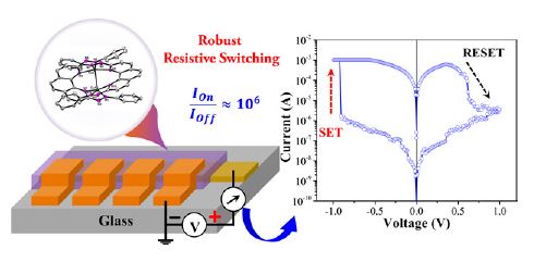
At the heart of Prof. Das’s memristor research is the phenomenon of resistive switching (RS) - the ability of a material or device to reversibly switch between different resistance states when subjected to an external voltage. Unlike traditional resistors that maintain a constant resistance, RS devices exhibit nonlinear and bistable I-V characteristics. At a critical voltage threshold, they "switch" from a high-resistance (OFF) state to a low-resistance (ON) state, and vice versa. This behavior is non-volatile, meaning the device retains its state even when the power is turned off.
Resistive switching is the foundational mechanism behind emerging Resistive Random-Access Memory (ReRAM), offering advantages such as:
• High switching speed (nanoseconds range)
• Low energy consumption
• Scalability to nanometer dimensions
• Potential for in-memory and neuromorphic computing
RS can be filamentary (localized conductive paths formed by ion migration or defect rearrangement) or interface-driven, depending on the material system and device configuration. The wide range of materials capable of RS - including oxides, organic films, chalcogenides, and 2D materials like MXenes - opens up vast possibilities for customizing device performance.
of bistable resistive switching device with the device schematic.
Part I: C-AFM for Memristor Innovation
One of the most intriguing parts of Prof. Das’s research focuses on RS in memristors—devices capable of toggling between multiple stable resistance states. These devices hold promise for data storage, logic operations, and neuromorphic computing.
The MXene Advantage
At the core of this work lies MXene, a family of two-dimensional materials derived from etching MAX-phase compounds. With high conductivity, mechanical strength, and tunable surface chemistry, MXenes are attractive candidates for memristive devices.
To fabricate these, Prof. Das’s group utilized a biphasic technique—depositing ultrathin films at the interface of two immiscible liquids, allowing better control over film uniformity and quality. Characterization using Raman spectroscopy and TEM confirmed the formation of high-quality 2D MXene sheets with clear D- and G-band features and a lattice spacing of 0.24 nm.
Visualizing Resistive Switching
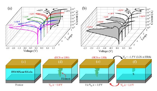
Using C-AFM, Prof. Das’s group probed local I-V characteristics of these MXene-based memristors. The results revealed:
• A SET process at +0.8 V, representing a switch to a high-conducting state.
• A RESET process upon reverse bias, bringing the device back to low conduction.
• Temporal response showing switching speeds of 30–45 nanoseconds, consuming just ~130–170 picojoules.
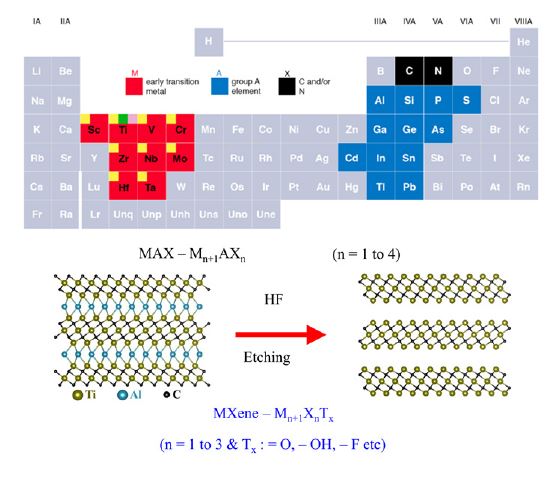
selective etching of aluminium atoms.
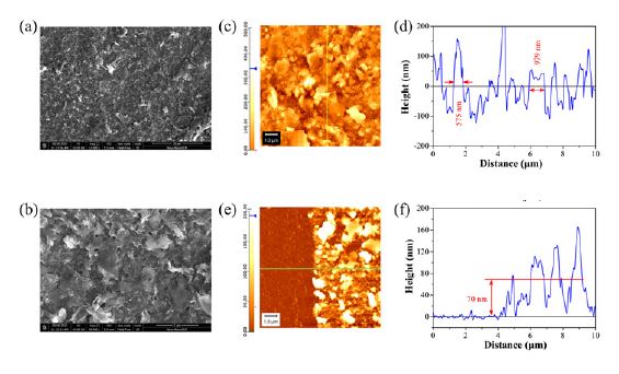
(Ti3C2TX) MXene nanoflakes visualized using scanning electron
microscope (SEM) and atomic force microscope (AFM).
Most significantly, C-AFM current mapping before and after voltage pulses provided direct visual evidence of filamentary conduction—a long-hypothesized yet rarely captured mechanism in RS. Post-SET images displayed a sharp increase in current confined to specific nanoscale regions, supporting the formation of conductive filaments.
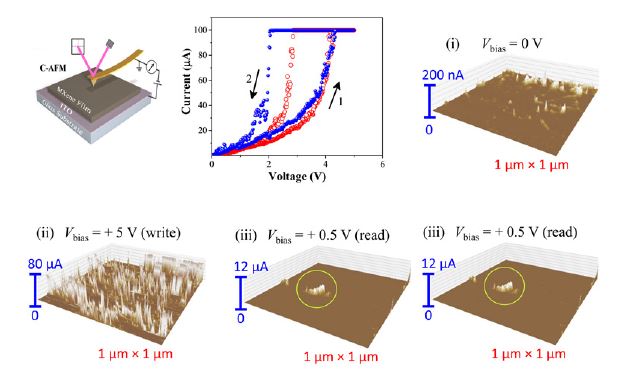
images at different applied bias voltages reveal resistive
switching behavior in the MXene film, indicating the
formation and rupture of filamentary conductive paths.
“This was the first time we directly visualized the conductive path formation and annihilation during RS in MXene thin film memristor device,” said Prof. Das, underscoring the unique capability of C-AFM in nanoscale device diagnostics.
Part II: KPFM for Self-Powered Photodetectors
In another segment of his talk, Prof. Das turned to Kelvin Probe Force Microscopy (KPFM)—an SPM variant sensitive to work function differences and contact potential variations.
Designing the Device
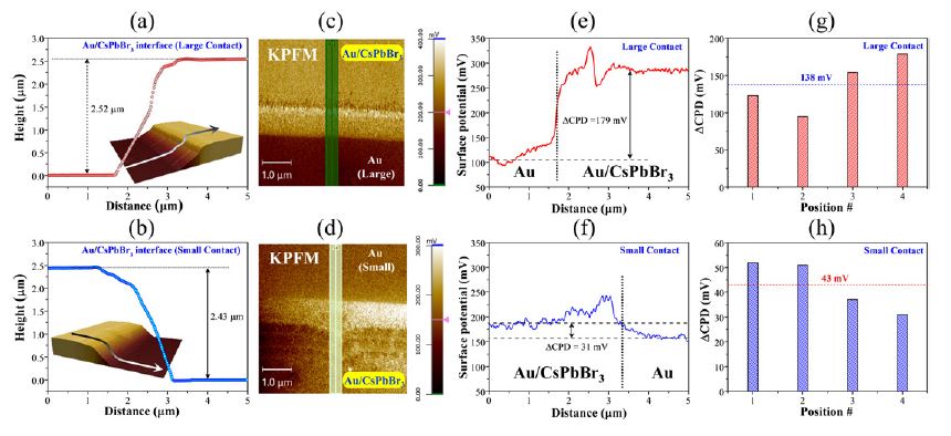
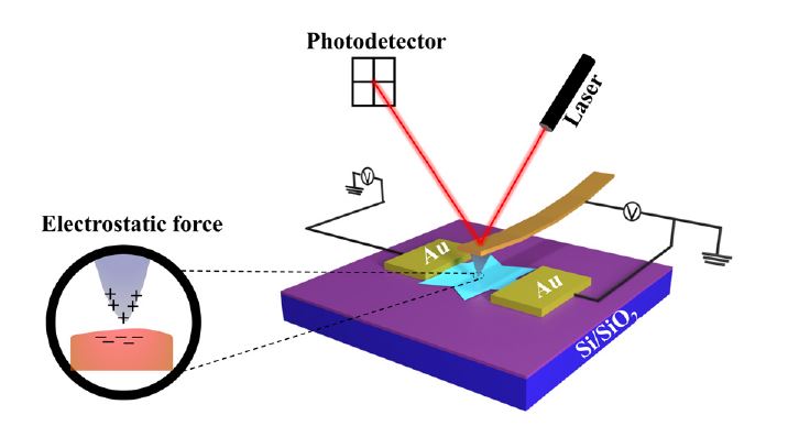
He described experiments using CsPbBr₃ perovskite crystals integrated into planar photodetector devices with symmetric Au electrodes. Surprisingly, even with identical electrode materials, the devices exhibited photovoltaic behavior—generating current under light without any external power.
The answer, he proposed, lies in asymmetric contact areas between the perovskite and each electrode. Crystals grown directly on one electrode surface had greater overlap, leading to distinct local work functions.
KPFM Validation
KPFM scans confirmed this hypothesis: the contact potential difference (CPD) was significantly higher at the larger contact area than at the smaller one, creating a built-in electric field sufficient to drive charge separation. This internal asymmetry allows the device to function in self-powered mode, an essential feature for low-power, next-gen sensors.
These findings, backed by meticulous electrical characterizations and modeling using Schottky barrier theory, were recently accepted for publication in Physical Review Applied.
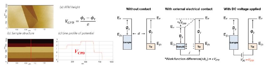
potential difference (CPD) across the sample surface.
interfaces.
Part III: EFM and the Role of Defects in 2D Semiconductors
Defects, especially grain boundaries (GBs), are inevitable in 2D material growth. Their impact on device performance—particularly in optoelectronics—is not fully understood. To address this, Prof. Das’s team used Electrostatic Force Microscopy (EFM) to probe monolayer MoS₂ flakes with controlled geometries and defects introduced during chemical vapor deposition (CVD) growth.
Optical and Electronic Signatures of GBs
• Raman and photoluminescence studies showed red shifts and line broadening at GBs, indicative of strain, defect states, and reduced band gaps.
• Devices fabricated with and without GBs showed stark performance contrasts. Devices without GBs exhibited ON/OFF ratios as high as 10⁵ and superlinear photocurrent response—suggestive of photothermal enhancement.
• Devices with GBs showed lower photocurrent and sluggish response times.
EFM Insights
EFM mapping under different sample bias conditions (+1 V, 0 V, –1 V) demonstrated charge puddling at GBs. These regions acted as potential barriers for both electrons and holes, suppressing carrier transport and increasing recombination. By correlating line profiles of electrostatic force variations with
device geometry, the group was able to visualize how GBs alter internal band structures and inhibit performance.
“This nanoscale visualization helps us understand how to engineer 2D material synthesis for better device outcomes,” said Prof. Das.
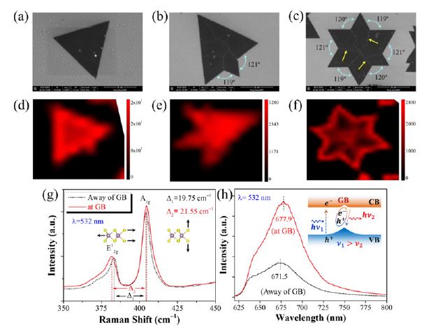
(GBs) to higher vertices. (A-C) SEM images. (D-F) Photoluminescence (PL) mapping images. (G and H) Raman scattering and PL spectra near and away of the GB, respectively.
A New Microscope, A New Horizon
A key enabler of this work has been the installation of a Park Systems NX7 AFM in Prof. Das’s lab. Since November 2023, this instrument has powered new modes of exploration—from ultrathin film thickness measurements to defect profiling and electrostatic analysis—underscoring the growing importance of advanced SPM platforms in electronic materials research.
Conclusion: SPM at the Crossroads of Nanotechnology and Functionality
Prof. Bikas C. Das’s lecture at the 2024 NanoScientific Symposium SE Asia highlights how advanced scanning probe microscopy is no longer a niche characterization tool—it is a strategic enabler of device innovation.
• C-AFM not only maps current but confirms conduction mechanisms at nanoscales.
• KPFM deciphers complex interface physics critical to self-powered optoelectronics.
• EFM reveals how defects modulate local fields and impact carrier dynamics.
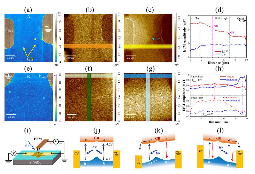
potential energy band diagrams corresponding to various testing conditions.
Together, these tools provide an integrated framework for understanding, designing, and optimizing future electronics. As we march toward neuromorphic computing, energy-efficient photodetectors, and high-performance 2D semiconductors, the insights delivered by SPM will remain indispensable.
And thanks to the vision of researchers like Prof. Das, the roadmap to this nanoscale frontier is becoming increasingly clear.


About Prof. Bikas C. Das
Dr. Bikas C. Das, Associate Professor at IISER Thiruvananthapuram’s School of Physics, leads a research group at the intersection of materials engineering and device physics. His team develops energyefficient electronic devices—such as memristors, memtransistors, and autonomous photodetectors—using advanced materials like 2D TMDs, halide perovskites, organic semiconductors, quantum dots, MXenes, and functional oxides. A central focus is neuromorphic hardware that mimics brain-like computing with fast response and ultra-low energy use, addressing the limits of CMOS-based systems. His work advances intelligent, adaptive, and sustainable electronics through innovative device design and material integration.
For more information, visit https://bikas.iisertvm.ac.in
