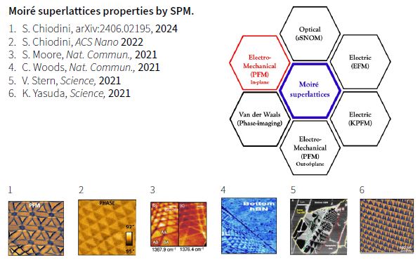
Revealing Twisted Realities: Mapping MoirÉ Superlattices In Hbn With Afm Phase Imaging
- 19 Aug 2025
- Volume 28
- NANOscientific Magazine, 2025
Dr. Stefano Chiodini, Italian Institute of Technology (IIT - Milan), Italy
Adapted from Presentation, Edited by NanoScientific
In the cutting-edge world of twistronics, where simple twists lead to revolutionary shifts in material properties, few phenomena are as visually and scientifically compelling as moiré superlattices. These striking nanoscale interference patterns, born from the rotational misalignment of two-dimensional (2D) materials, have captivated physicists and material scientists alike. At the 2024 NanoScientific Forum Europe, Dr. Stefano Chiodini of the Instituto Italiano di Tecnologia presented an elegant, experimentally robust method for visualizing and characterizing these moiré patterns in twisted hexagonal boron nitride (t-hBN)—using atomic force microscopy (AFM) in an inventive phase imaging modality.
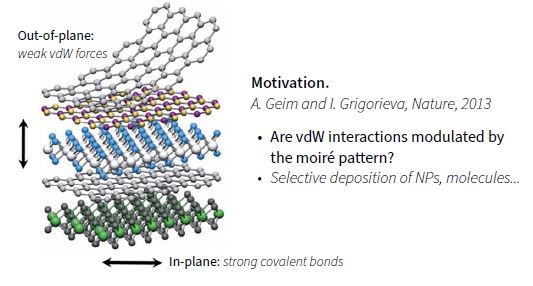
This groundbreaking work, funded by the ERC CoG “METAmorphoses” and achieved as collaborative effort between the groups of Dr. Antonio Ambrosio at IIT Milano and Prof. Andrea Ferrari at University of Cambridge, not only deepens our understanding of interlayer van der Waals (vdW) interactions in layered materials, but also uncovers a surprising new aspect of moiré physics: in-plane polarization patterns that extend the complexity of known electromechanical responses. His findings offer new frontiers for nano-engineered materials, where atomic misalignments may one day be tailored for advanced photonic, electronic, and quantum devices.
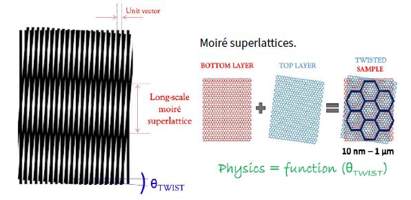
Twistronics: When Geometry Transforms Physics
Twistronics refers to the manipulation of electronic properties through the deliberate twisting of atomically thin materials like graphene or hBN. A small twist angle—often less than 1°—between two stacked layers of such materials creates a long-range periodic pattern, or moiré superlattice. This geometrical trick, deceptively simple, unlocks entirely new physical behaviors by altering interlayer couplings and symmetries.
As Dr. Chiodini explains, “The entire physics of your twisted sample becomes a function of the twist angle. With no chemical modifications, just geometric control, you can induce entirely new material properties.”
This was famously demonstrated in 2018, when twisted bilayer graphene at the “magic angle” of ~1.1° was found to exhibit superconductivity. But the concept is not limited to graphene. In layered insulators like hBN, moiré patterns have been shown to modulate optical, electrical, and electromechanical properties—manifesting as triangular domains in near-field, Kelvin probe, and piezoresponse force microscopy.
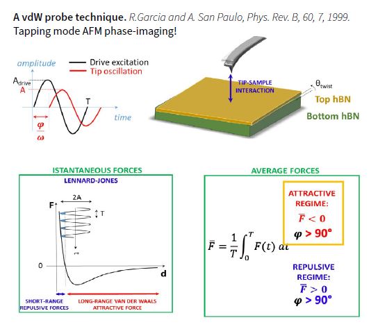
AFM Phase Imaging: A Van der Waals Interaction Microscope
While previous work explored moiré-induced modulations in surface potential
and piezoelectricity, Chiodini’s team posed a novel question: Are van der Waals interactions themselves modulated by the moiré pattern?
To probe this, they turned to an unexpected ally: AFM phase imaging in tapping mode. This well-established technique, often used to infer material stiffness or energy dissipation, can also act as a sensitive detector for vdW forces when configured in the attractive regime.
“In tapping mode,” Chiodini notes, “the phase lag between the cantilever’s oscillation and the drive signal reveals the nature of tip-sample interactions. If the average interaction is attractive, dominated by van der Waals forces, the phase exceeds 90°.”
By tuning the AFM to operate in this vdW-sensitive regime, Chiodini and his collaborators could map out the local interaction energy landscape without applying voltage or making contact—ideal for delicate 2D materials. Remarkably, they discovered a spatial modulation of the phase signal that mirrored the moiré lattice itself.
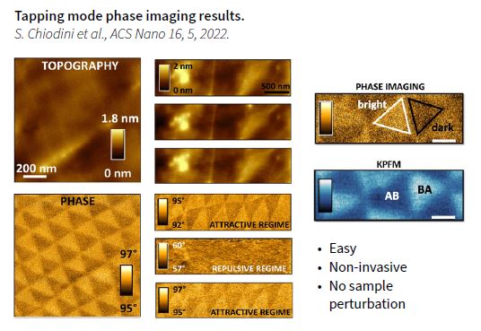
Images of twisted hBN revealed familiar triangular domains—absent in topographic scans but vividly apparent in phase contrast, confirming a direct correlation between moiré geometry and vdW interaction strength.
“This approach is non-invasive, requires no conductive tip or substrate, and avoids sample perturbation,” Chiodini emphasizes. “It’s a powerful, underutilized way to image moiré physics.”
Electromechanical Depth: From Out-of-Plane to In-Plane Polarization
In the second part of his presentation, Chiodini ventured into less-charted territory: in-plane electromechanical responses of moiré-patterned hBN. While prior work had demonstrated out-of-plane polarizations in AB and BA stacking domains—arising from slight shifts in atomic registry—Chiodini hypothesized the existence of in-plane dipoles, forming a more intricate 3D polarization lattice.
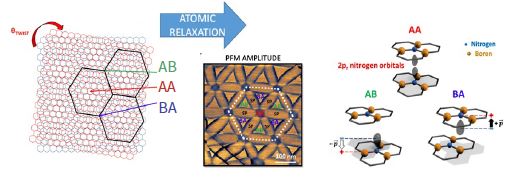
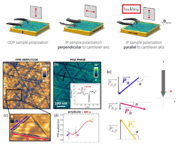
To probe this, his team used vertical piezoresponse force microscopy (V-PFM), exploiting a subtle phenomenon known as the “buckling effect.” While V-PFM typically detects vertical motion due to out-of-plane polarization, it can also register cantilever buckling when an in-plane polarization vector aligns with the cantilever axis.
“In this buckling geometry, the cantilever bends vertically due to in-plane forces, and the photodiode detects a vertical signal just as if there were out-of-plane motion,” he explains. “But it’s really the in-plane polarization being picked up.”
By analyzing amplitude signals along different edges of the triangular moiré domains—each corresponding to a different orientation—Chiodini's team observed a sinusoidal dependence of amplitude on the angle between polarization vector and cantilever axis. When the edge aligned with the cantilever axis (90° projection), the buckling signal peaked. This angular modulation is a direct fingerprint of in-plane dipole activity.
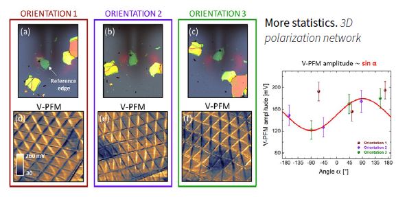
To strengthen their case, the researchers reoriented the same hBN flake in multiple directions relative to the cantilever and repeated the measurements. Each time, they mapped nine distinct domain edges with consistent sinusoidal trends, providing compelling statistical evidence of in-plane polarization.
This work marks the first demonstration of in-plane polarization in t-hBN moiré superlattices, enriching the previously one-dimensional picture of electromechanical behavior. “We are looking at a true 3D polarization network,” Chiodini concluded. “This opens new questions about the internal field distributions and their coupling to external stimuli.”
Implications and Future Directions
The implications of Chiodini’s dual discoveries—the modulation of vdW forces and the existence of in-plane polarization—are far-reaching. First, they suggest that even fundamental interatomic interactions are sensitive to geometric phase effects in layered materials. This could influence how nanoparticles, molecules, or even atoms selectively adsorb on such surfaces, enabling directed self-assembly on a moiré template.
Second, the observation of multidirectional polarization fields invites a rethinking of piezoelectric and ferroelectric applications in 2D materials. Could twist-controlled dipole architectures be used in nanoscale transducers, energy harvesters, or logic elements? What role might they play in light-matter interactions or topological excitations?
Moreover, Chiodini’s results serve as a call to revisit older AFM techniques under a new theoretical lens. Phase imaging—often sidelined in favor of more quantitative methods—has shown its value as a highly sensitive, artifact-free probe for subtle nanoscale phenomena.
Final Reflections
Dr. Chiodini’s meticulous and creative approach demonstrates the continued relevance of fundamental scanning probe microscopy in frontier physics. His ability to extract profound insights from familiar tools speaks to the evolving interplay between instrumentation and imagination in nanoscience.
At a time when quantum materials and flat-band phenomena are reshaping electronics, understanding the hidden landscapes of interlayer interactions and internal fields becomes crucial. Twisting hBN is no longer just a geometrical curiosity—it is a platform for engineering the invisible forces that shape the future of materials.
As twistronics matures from serendipity to design, Chiodini’s work lights the path with clarity, rigor, and just the right angle.

Dr. Chiodini is a researcher in the Vectorial Nano- Imaging Group at the Italian Institute of Technology, where since July 2020 he has been
using scanning probe microscopy to investigate the optical, electronic, and mechanical properties of twisted 2D materials, small molecules,
and polymers. From 2017 to 2019, he was a postdoctoral fellow in the PLATON group at the University of Zaragoza, contributing to the MAGIC
CELL GENE project with AFM-based studies of cell membranes and self-assembled molecular electronics. Prior to that, he worked as a postdoc
at ICMM-CSIC in Madrid starting in 2015, focusing on atomic-scale studies of metal-organic frameworks and advancing techniques in atomic-resolution and multifrequency AFM. He earned his
PhD in Physics in 2015 from the National Research Council (ISMN-CNR) in Bologna, where his research under Prof. Fabio Biscarini centered
on the growth of organic semiconductors using real-time AFM in UHV. He received his bachelor’s and master’s degrees cum laude from the University of Bologna in 2010.
For more information on the work, funding and
research groups involved, please visit:
https://pubs.acs.org/doi/10.1021/acsnano.1c11107
https://pubs.acs.org/doi/10.1021/acsnano.4c12315
https://www.iit.it/web/vectorial-nano-imaging
https://ercmetamorphoses.eu/
http://www-g.eng.cam.ac.uk/nms/home.html
Category