Unveiling The True Shape Of Conductive Filaments: Adaptive Scalpel Spm Redefines 3d Volumetric Sensing
- 18 Aug 2025
- Volume 28
- NANOscientific Magazine, 2025
Poster Winner at NanoScientific Symposium Americas 2024
Md Ashiqur Rahman Laskar and Team, Arizona State University
Adapted from Presentation, Edited by NanoScientific
In the nanoscopic realm of advanced materials and electronic devices, precision is everything. The need to understand, control, and characterize structures at the nanoscale has driven the evolution of microscopy into a high-art of engineering and physics. At the 2024 NanoScientific Symposium, Researcher Md Ashiqur Rahman Laskar and his interdisciplinary team from Arizona State University, INRiM (Italy), and Neno-Vision (Czech Republic) presented an award-winning breakthrough in this domain—Adaptive Scalpel Scanning Probe Microscopy (SPM), a transformative approach to three-dimensional tomographic analysis. This work addresses a longstanding issue in conductive atomic force microscopy (C-AFM): the parasitic effects caused by tip-sample junction leakage and inhomogeneous electric fields, which distort lateral and vertical resolution in 3D reconstructions. Laskar’s innovation offers a path to sub-1000 nm³ tomographic precision, especially for characterizing resistive switching memories—ushering in a new era of volumetric sensing in nanoelectronics.
The Problem: Artifacts in Nanoscale Tomography
At the heart of modern nanoelectronics lies a growing class of devices that rely on resistive switching—such as valence change memory (VCM) systems based on transition metal oxides like NbOx. These systems depend on the reversible formation and rupture of nanoscale conductive filaments (CFs), which define the ON and OFF states of a memory cell. Understanding these filaments, including their 3D morphology and evolution, is critical for optimizing device performance and longevity.
Yet a key barrier to true 3D insight has been tip-induced artifacts in conventional tomographic atomic force microscopy. These artifacts fall into two primary categories:
-
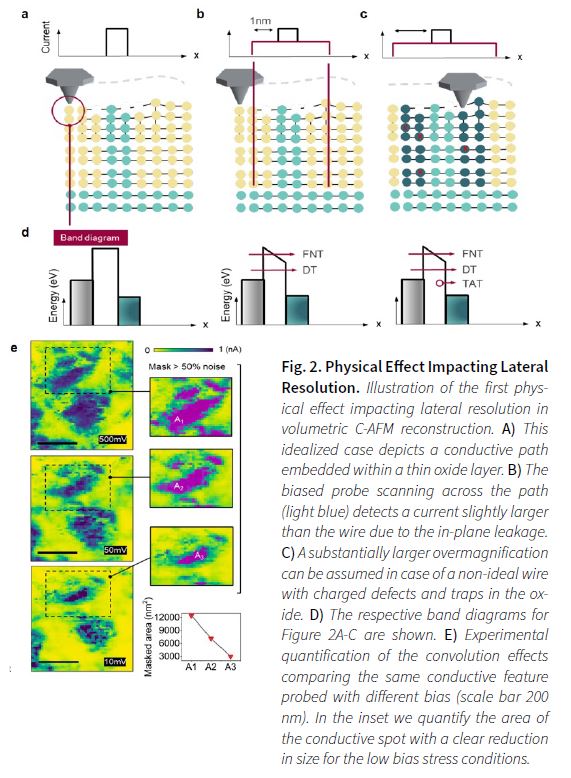
In-plane leakage: Current spreads laterally due to parasitic conduction pathways through the surrounding oxide matrix. As a result, the detected current footprint significantly overestimates the actual lateral dimensions of the conductive feature (i.e., the CF).
-
Vertical overbiasing: As material is removed layer by layer during the tomographic process, the oxide thickness reduces, causing an unintentional increase in electric field strength. This non-uniformity leads to variations in contrast and feature depth, skewing vertical resolution.
The result? A bloated and blurred picture of what should be nanosharp and sharply localized.
The Innovation: Adaptive Scalpel SPM
To combat these dual distortions, Laskar’s team devised Adaptive Scalpel SPM, an approach that dynamically adjusts the tip-sample bias throughout the tomographic process. Instead of applying a constant voltage, which leads to uncontrolled increases in electric field as oxide layers thin, the adaptive method calibrates the bias to maintain a steady internal electric field—thus preserving contrast integrity as depth increases.
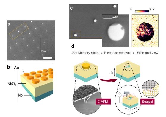
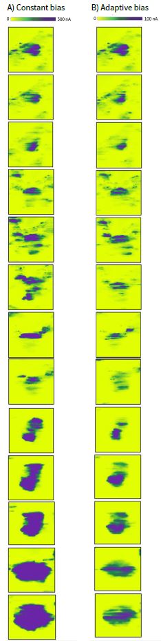
This innovation was tested on VCM cells with gold (Au) top electrodes and NbOx-based switching layers. After removing the Au layer (see Fig. 1), a sharp conductive probe was used to iteratively erode the NbOx material while mapping current flow. Two acquisition modes were compared:
• Constant bias mode: Fixed voltage during the entire scalpel scan.
• Adaptive bias mode: Voltage tuned according to oxide thickness to stabilize the internal electric field.

Uncovering the True Filament Geometry
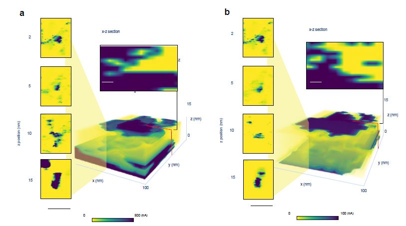
The difference between these two approaches is vividly captured in 3D volumetric reconstructions of the conductive filament. Under constant bias, the filament appears larger and less defined, a result of leakage spreading and overbiasing. In contrast, adaptive bias yields a filament image that is smaller, sharper, and more confined—closely matching theoretical expectations and physical models.
This is reinforced in the cross-sectional comparisons of x-y and x-z slices, where the adaptive bias captures a sharply bounded filament located precisely at the core of the active device area. Such precision is crucial when designing or troubleshooting high-density memory arrays or emerging logic components and improved resolution.
Quantitative Insights: Resolution and Leakage Control
The experimental data quantifies the improvement.
- Lateral resolution improves due to reduced in-plane leakage, confirmed by varying the bias during scanning and observing a clear decrease in current footprint size.
- Vertical sensitivity is optimized through adaptive voltage control, leading to significant decrease in vertical leakage and charging artifacts.
• An adaptive tip-sample biasing scheme is demonstrated for reduction
in overestimation of the lateral dimensions and the mitigation of a class of artefacts induced by the high electric field inside the thin oxide when volumetrically reduced.
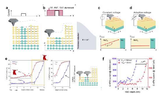
the oxide progressively. C) As the oxide thickness is reduced, the internal electric field will rise during the measurement. D) The concept of adaptive scalpel SPM is to maintain a constant electric field during the analysis by adjusting the tip-sample bias as the oxide is made thinner. E) Evolution of the tip-sample current as a function of depth for a CF (red) and pristine oxide (blue). In the inset, we show the schematic
of the acquisition area. F) The evolution of the tip-sample current for a pristine oxide region compares the leakage in the case of constant bias (blue) and adaptive bias (red).
Fig. 2 provides an instructive visualization of in-plane leakage effects, while Fig. 3 explains how thickness-dependent field increases can distort vertical profiling. The adaptive bias strategy not only restores fidelity but allows for reliable current-depth analysis, further substantiating its effectiveness.
Beyond Resistive Memories: Broader Impact
Although this study focuses on NbOx-based VCM cells, the implications of Adaptive Scalpel SPM stretch far beyond memory technology. In photovoltaics, 3D conductive networks and ion migration paths are critical to device stability and efficiency. In ferroelectrics and piezoelectrics, understanding charge domain structures and their evolution during operation demands similar volumetric precision. In 2D and layered devices, heterostructures such as transition metal dichalcogenides or perovskite-based architectures require reliable tomography to decode buried interface physics. By enabling 3D reconstructions with sub-1000 nm³ resolution, Adaptive Scalpel SPM positions itself as a universal tool for high-precision electrical nanocharacterization.
Practical Implementation: Tip-Device Interface
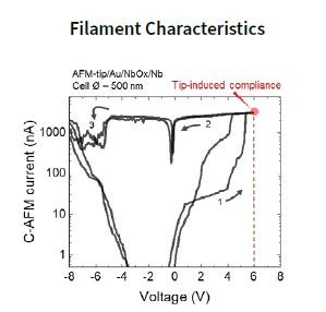
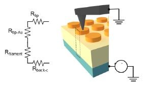
A detailed understanding of the tip-sample interaction was also key to the study. As the schematic in Fig. 7 shows, the team modeled the tip-Au-NbOx stack as an equivalent resistive network. Once the Au top electrode is removed, the tip-sample junction becomes the primary resistance limiter. This naturally introduces a form of current compliance, a fortunate artifact that protects the device from damage during scanning.
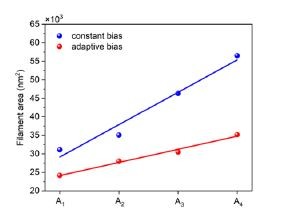
Moreover, I-V curves demonstrate stable switching characteristics, and consistent current evolution under adaptive bias indicates improved reproducibility. Notably, Fig. 8 reveals that the filament area measured at the deepest slices of the NbOx device was significantly smaller in adaptive mode, confirming better spatial confinement.
Collaboration and Outlook
This project is a testament to international scientific collaboration. Co-authors from ASU, INRiM, and NenoVision brought together expertise in materials science, metrology, AFM technology, and device engineering. The equipment and infrastructure support of ASU’s Eyring Materials Center and funding from DOE and NSF were critical to its success. Looking ahead, Laskar and his colleagues envision integrating adaptive scalpel techniques into broader AFM platforms, potentially in combination with machine learning algorithms for automated reconstruction and classification of 3D features. The goal is clear: bring unprecedented clarity and confidence to nanoscopic tomography.
Conclusion
The work of Md Ashiqur Rahman Laskar and his team exemplifies the spirit of NanoScientific: combining creativity, technical mastery, and scientific rigor to break new ground in nanoscale exploration. Their Adaptive Scalpel SPM approach not only solves a real and pressing problem in AFM tomography, it redefines the resolution standards for the entire field. As nanoscale systems become ever more complex, tools like Adaptive Scalpel SPM will be essential in decoding their structure-function relationships, helping engineers build the next generation of smart, efficient, and responsive devices.

Md Ashiqur Rahman Laskar is a PhD candidate in Electrical Engineering
at Arizona State University (ASU), specializing in semiconductor
metrology and failure analysis. He is doing research with Dr. Umberto
Celano at ASU. The ASU team aims to design experiments and develop
advanced metrology techniques for the emerging devices and
materials. The research goal is to understand and observe the fundamental processes that govern the operation of emerging devices,
through nanoscale analytical imaging and correlative metrology. This
generates fundamental understanding to engineer improved materials
for nanoelectronics. The ASU team behind the research: PhD students A. Laskar, S. Chakrabarti; Prof. U. Celano, the principal investigator of Nanoelectronics Metrology & Failure Analysis Lab at ASU.
For more information, https://labs.engineering.asu.edu/celano/
From L-R: Md Ashiqur Laskar, Srijan Chakrabarti, Dr. Umberto Celano
References
• M. A. R. Laskar, G. Leonetti, G. Milano, O. Novotný, J. Neuman, S. Tongay, U.
Celano, Adaptive Scalpel Scanning Probe Microscopy for Enhanced Volumetric
Sensing in Tomographic Analysis. Adv. Mater. Interfaces 2024, 11, 2400187.
• Song, J., Zhou, Y., Padture, N.P. et al. Anomalous 3D nanoscale photoconduction in hybrid perovskite semiconductors revealed by tomographic atomic force microscopy. Nat Commun 11, 3308 (2020).