Unlocking Advanced Material Insights With Imaging Spectroscopic Ellipsometry
- 04 Nov 2025
- Volume 29
- NANOscientific Magazine, 2025
Dr. Mangesh Diware, Park Systems Inc.
Adapted from Presentation, Edited by NanoScientific
Introduction: A New Dimension in Ellipsometry
At the 2024 NanoScientific Symposium, Dr. Mangesh Diware took the audience on a journey through one of the most powerful—and evolving—optical metrology techniques in nanoscience: Imaging Spectroscopic Ellipsometry (ISE). Building on the robust foundations of traditional ellipsometry, ISE integrates high-resolution imaging to evaluate not only thickness and refractive index, but also spatially resolved optical property variations at the micron scale.
Ellipsometry has been a cornerstone in materials science for decades, delivering non-contact, non-destructive characterization of thin films and layered structures. But the challenge has always been lateral resolution, limited by focusing optics. Conventional ellipsometry averages data over tens of microns. ISE changes that—fusing the vertical precision of ellipsometry (down to 0.1 nm) with lateral resolution of approximately 1 µm.
As Dr. Diware described, “The integration of imaging opens entirely new possibilities—seeing not just the average behavior, but the local variations that matter in devices and advanced material science.”
Ellipsometry: From the Dark Ages to Imaging Era
The origins of ellipsometry stretch back to the foundational work of Robert Hooke and James Clerk Maxwell. The technique’s modern development can be viewed in three stages [1]:
• Dark ages – Before digital electronics, measurements relied on nulling methods, manually adjusting optics until no light was detected. Analysis was slow and highly operator dependent.
• Modern age – The 1970s brought photometric designs and the first computer-controlled systems (notably by Aspens and Sudana), allowing automated data collection.
• Postmodern era – The introduction of photodiode arrays and spectroscopic scanning enabled fast, multi-wavelength acquisition. A 2013 innovation—the three-polarizer configuration—eliminated the wavelength dependence of older compensators.
These advances established ellipsometry as a high-precision optical tool. However, as device geometries shrank and structures grew more complex, the need for lateral resolution became increasingly critical, setting the stage for ISE.
The Physics Behind Ellipsometry: Why Phase Matters
Ellipsometry works by measuring how the polarization of light changes after interaction with the sample surface. Specifically, it tracks the change in amplitude ratio (Ψ) and phase (Δ) between two orthogonal components of the electric field (parallel and perpendicular to the plane of incidence).
Phase sensitivity is key. Even a 0.01° shift in phase can correspond to changes in thickness on the femtometer scale. In practice, ellipsometry can detect sub-nanometer thickness differences. Use of different spectral ranges helps to probe different physical properties.
• UV–Visible – Band structure, band gap energies, excitonic features, and crystalline order.
• Infrared – Carrier concentrations, mobilities, and phonon behavior. This versatility makes ellipsometry valuable across semiconductors, photovoltaics, and 2D materials.
Modeling: Turning Ψ and Δ into Physical Insight
One of ellipsometry’s defining features is its reliance on modeling. Raw Ψ–Δ spectra contain all the necessary information about the sample.
However, to extract the desired material properties, the data must be modeled using a multilayer structure that closely represents the actual sample.
Modeling typically involves:
• Defining layer structure (substrates, thin films, interfaces, roughness layers)
• Using known or estimated optical constants (n, k)
• Iteratively refining fits against measured spectra
The process can be complex, but it is precisely this step that allows ellipsometry to extract high-value information—layer thicknesses, dielectric
functions, roughness, and even multi-layer film stacks. Dr. Diware noted that while modeling is sometimes seen as a barrier, it is actually a powerful interpretive tool: “If your model is accurate, it will give you insights beyond what direct measurements can show.”
The Leap to Imaging Spectroscopic Ellipsometry (ISE)
Traditional ellipsometry measures an averaged response over a spot size ~50 µm or larger. For shrinking devices structures, this is a limitation: local variations are invisible.
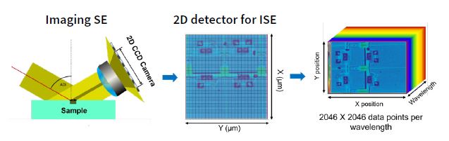
ISE solves this by replacing the point detector with a 2D camera. Every pixel becomes a detector, providing localized Ψ and Δ values (see Fig. 1). Lateral resolution can reach 1 µm while vertical resolution remains at ~0.1 nm.
In practical terms, ISE can collect millions of spectra in a single scan, producing full-field maps of optical properties. This is crucial for patterned wafers, 2D materials, and non-uniform coatings.
Applications: From 2D Materials to Real-Time Electrochemistry
Dr. Diware highlighted several applications where ISE is transformative:
-
2D Materials & Heterostructures
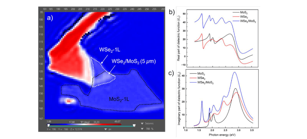
ISE excels in characterizing atomically thin materials such as MoS₂ [2,3], WS₂ [4], and graphene [5]. By mapping Ψ–Δ pixel-by-pixel, ISE can distinguish monolayer, bilayer, and trilayer regions and extract anisotropic dielectric properties. In one example, a MoS₂ flake on 300 nm SiO₂/Si was mapped in a single field of view—substrate, flake, and thickness variations all captured simultaneously.
2. Patterned and Microstructured Surfaces
ISE can resolve optical property variations across lithographically patterned surfaces, including variations at edges and interfaces. This is vital for advanced electronics and photonics manufacturing, where uniformity at the micro-scale is critical.
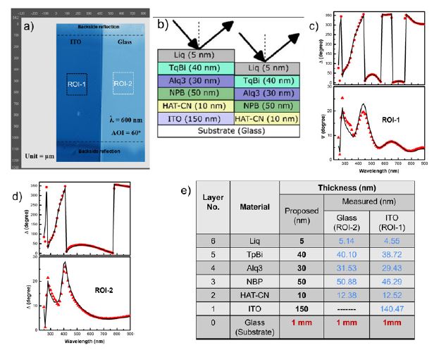
3. Transparent Substrates & Knife-Edge Illumination
Backside reflections pose a significant challenge when working with transparent substrates such as glass. Park Systems addresses this with a knife-edge illumination setup that blocks half the beam, eliminating backside noise. This allows accurate measurements even on low-cost substrates.
4. Ellipsometric Contrast Microscopy (ECM)
For rapid visualization, ECM mode within ISE optimizes polarizer/analyzer angles to enhance contrast of low-optical-contrast features [5]—making monolayer flakes visible even on plain glass substrates without expensive oxide-coated wafers.
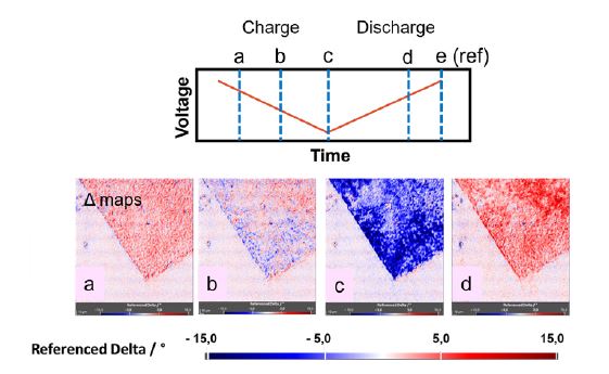
5. Real-Time Monitoring of Intercalation Processes
ISE can investigate dynamic processes, such as sodium-ion intercalation
in Janus graphene. Fig. 4 shows the operando observation of Δ shifts, enables researchers to monitor ions moving in and out of layered structures in real time — providing unprecedented insight into electrochemical processes vital to energy storage [6, 7].
Technical Framework: Anatomy of an ISE System
An ISE setup includes:
• Polarizer and compensator for controlling incident polarization
• High-precision sample stage under a microscope objective
• 2D photodiode, CCD or CMOS camera for pixel-resolved detection
During measurement, the compensator is rotated, and at each step the camera captures intensity maps. From these, Ψ and Δ maps are calculated. Full-field data can be analyzed as a whole or divided into regions of interest (ROI) for targeted modeling.
In display research, for example, a single scan of a pixel cell can be subdivided into RGB subpixel regions, each modeled separately—without rescanning.
Case Study: MoS₂ Anisotropy
One striking example involved MoS₂ exfoliated onto a SiO₂/Si substrate. ISE captured the full flake in one scan. Modeling revealed strong in-plane (x-y) excitonic peaks (A and B excitons) and absence of such peaks along the out-of-plane (z-axis) direction, consistent with confinement effects. The measured birefringence exceeded 2.5—among the highest reported [3]. Such anisotropy has direct implications for integrating 2D materials into photonic devices and hybrid optoelectronic–photonic circuits.
Why ISE Matters: A Researcher’s Perspective
ISE is more than just an incremental improvement in ellipsometry—it fundamentally changes the scale and nature of the analysis:
• Non-contact & Non-destructive – Ideal for delicate films and functional devices.
• Vertical & Lateral Resolution – Sub-nanometer vertical sensitivity combined with micron-scale lateral mapping.
• Throughput & Efficiency – Millions of spectra captured per scan, enabling rapid evaluation of complex samples.
• Interpretive Power – Model-based analysis transforms optical data into physical, structural, and functional understanding.
As Dr. Diware concluded, “If you have a research problem and no solution in sight, imaging ellipsometry might be the key.”
Conclusion: Expanding the Reach of Optical Metrology
With Imaging Spectroscopic Ellipsometry, Park Systems is redefining what optical metrology can deliver. From single layer 2D materials to multi-layer OLED stacks, from transparent substrates to real-time electrochemistry, ISE combines precision, versatility, and efficiency. Its capacity to map both thickness and optical properties at high lateral resolution opens entirely new avenues for understanding and engineering advanced materials. ISE is not just the next step in ellipsometry—it is becoming an indispensable tool in the expanding frontier of nanoscience and technology.
Dr. Mangesh Diware is a Senior Application Scientist at Park Systems Inc., California. He holds dual master's degrees—one in Physics from Nagpur University (2006) and another in Materials Engineering from Visvesvaraya National Institute of Technology (VNIT), India (2009). He earned his Ph.D. in Physics from Kyung Hee University, South Korea, in 2014 under the guidance of Prof. Young Dong Kim. From 2014 to 2017, Dr. Diware worked as a Senior Research Scientist at the Korea Research Institute of Standards and Science (KRISS), where he focused on developing ultrathin film metrology techniques. In 2018, he joined Seoul National University as a Research Associate, conducting advanced optical spectroscopy studies on quantum materials.
With over a decade of experience in materials science and optical spectroscopy, Dr. Diware specializes in exploring material properties using light-based techniques, particularly spectroscopic and imaging ellipsometry. His work contributes to advancements in semiconductors, flexible electronics, and next-generation display technologies. His accolades include the Presidential Fellowship, a Postdoctoral Fellowship from KRISS, and the “Best Researcher of the Year” award at KRISS.
References
-
Aspnes, D. E. (2014). Spectroscopic ellipsometry – Past, Present, and Future, 571 (3), 334.
-
Funke, S., Miller, B., Parzinger, E., Thiesen, P., Holleitner, A. W., & Wurstbauer, U. (2016). Imaging spectroscopic ellipsometry of MoS₂. Journal of Physics: Condensed Matter, 28 (38), 385301.
-
Ermolaev, G. A., Grudinin, D. V., Stebunov, Y. V., Voronin, K. V., Kravets, V. G., Duan, J., Mazitov, A. B., Tselikov, G. I., Bylinkin, A., Yakubovsky, D. I., Novikov, S. M., Baranov, D. G., Nikitin, A. Y., Kruglov, I. A., Shegai, T., Alonso-González, P., Grigorenko, A. N., Arsenin, A. V., Novoselov, K. S., & Volkov, V. S. (2021). Giant optical anisotropy in transition metal dichalcogenides for next-generation photonics. Nature Communications, 854 (12), 1.
-
Wurstbauer, U., Röling, C., Wurstbauer, U., Wegscheider, W., Vaupel, M., Thiesen, P. H., & Weiss, D. (2010). Imaging ellipsometry of graphene. Applied Physics Letters, 97 (23), 231901.
-
Sigger, F., Lambers, H., Katharina, N., Klein, J., Saigal, N., Holleitner, N. W., & Wurstbauer, U. (2022). Spectroscopic imaging ellipsometry of two-dimensional TMDC heterostructures. Applied Physics Letters, 121 (7), 071102.
-
Sun, J., Sadd, M., Edenborg, P., Grönbeck, H., Thiesen, P. H., Xia, Z., ... & Palermo, V. (2021). Real-time imaging of Na⁺ reversible intercalation in “Janus” graphene stacks for battery applications. Science Advances, 7 (22), eabf0812.
-
Okano, S., Sharma, A., Ortmann, F., Nishimura, A., Günther, C., Gordan, O. D., ... & Zahn, D. R. (2020). Voltage-controlled dielectric function of bilayer graphene. Advanced Optical Materials, 8 (20), 2000861.