From Non-Contact AFM to Functional Nanoscopy Expanding the Capabilities of Scanning Probe Microscopy
- 21 May 2026
- Volume 30
- NANOscientific Magazine, 2026
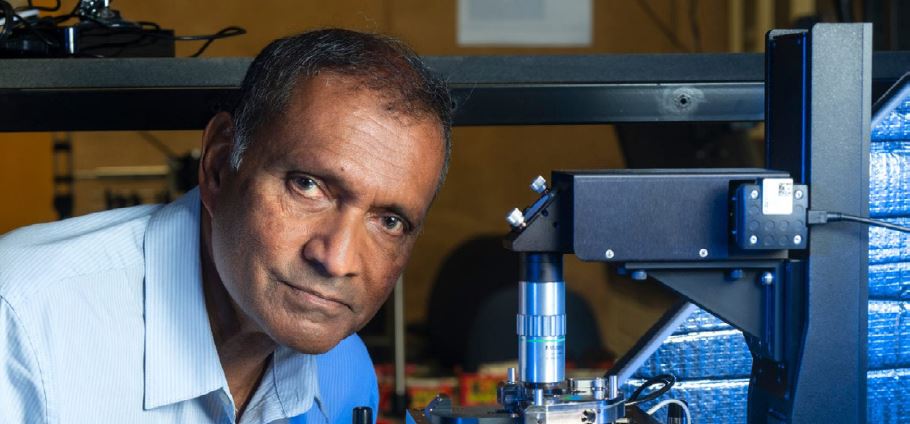
Prof. Kumar Wickramasinghe, UCI Distinguished Professor Emeritus, Henry Samueli Endowed Chair Emeritus, University of California, Irvine, CA, USA
Introduction
Over the past four decades, atomic force microscopy has evolved from a surface imaging tool into a versatile platform for nanoscale characterization. Beyond topography, AFM now enables measurement of electrical, magnetic, thermal, and optical properties with high spatial resolution.
This transformation was driven by the need to understand functionality at the nanoscale, particularly in semiconductor manufacturing and advanced materials research. As presented by Kumar Wickramasinghe at the Stanford NanoScientific Symposium, key developments—including non-contact AFM and a range of functional scanning probe techniques—expanded AFM into a comprehensive measurement platform, laying the foundation for modern functional nanoscopy.
Early Motivation: Nanoscale Metrology
In the early 1980s, semiconductor feature sizes were approaching the limits of optical microscopy, creating an urgent need for higher-resolution metrology. Feature sizes in microelectronics and magnetic storage were approaching half a micron, and further progress would require new measurement tools capable of resolving structures an order of magnitude smaller.
At IBM Research, efforts were underway to explore scanning probe approaches that could address these emerging metrology challenges. One early concept investigated by Wickramasinghe’s group was a scanning thermal microscope, in which a heated probe tip approached a cooler sample surface. Heat transfer between the tip and the sample served as an indicator of their separation. As the tip moved closer to the surface, thermal conduction increased, causing the probe temperature to drop more rapidly.
Although this technique successfully demonstrated nanoscale surface profiling on insulating materials, the spatial resolution achieved—on the order of several hundred angstroms—was insufficient for semiconductor manufacturing requirements. As device dimensions continued to shrink, resolutions of tens of angstroms were needed.
Around this time, the publication of the AFM introduced a new approach that promised significantly higher resolution and broader applicability.
Toward Non-Contact Atomic Force Microscopy
Early AFM instruments typically operated in contact mode, in which the probe tip maintained direct contact with the surface while scanning. While effective for measuring topography, contact operation could disturb or damage delicate surfaces and nanoscale structures.
To overcome these limitations, researchers began exploring methods for operating AFM without direct contact between the tip and the sample. A key step involved oscillating the cantilever near its resonance frequency while monitoring extremely small changes in its vibration behavior.
Using highly sensitive optical detection methods, including laser heterodyne probes capable of detecting minute vibrations, researchers could observe how the cantilever’s oscillation changed as it approached a surface. Long-range attractive forces—primarily van der Waals interactions—alter the effective stiffness of the cantilever and cause shifts in its resonance frequency.
By monitoring these shifts and maintaining constant oscillation conditions through feedback control, the microscope could operate with the tip positioned extremely close to the surface without touching it. This approach became known as non-contact AFM, enabling stable imaging while minimizing tip wear and sample damage.
Early experiments achieved spatial resolutions on the order of five nanometers, already sufficient for many metrology applications envisioned by semiconductor manufacturers.
Engineering AFM for Manufacturing Environments
Demonstrating nanoscale imaging in a research laboratory was only the first step. For scanning probe microscopy to become useful in semiconductor fabrication, it had to be engineered into a robust and automated measurement system capable of handling large wafers with high reliability.
This presented a formidable engineering challenge. The probe tip, typically about one hundred micrometers long, must be controlled with nanometer precision while scanning across surfaces thousands of times larger than the tip itself. Maintaining stable operation under these conditions required innovations in both instrumentation and automation.
Key developments included microfabricated silicon cantilevers with integrated sharp tips, automated tip-exchange mechanisms, dual feedback control systems for maintaining stable tip–sample spacing, and robotic wafer handling systems capable of loading and positioning semiconductor wafers for measurement.
These advances made it possible to build scanning probe workstations capable of performing nanoscale measurements directly within semiconductor manufacturing environments. One early application involved diagnosing failures in integrated circuits caused by subtle variations in chemical-mechanical polishing processes. AFM measurements revealed nanoscale topographic variations that were invisible to optical inspection methods, allowing engineers to identify and correct the underlying process issues.
This transition marked an important milestone in the history of scanning probe microscopy, demonstrating that AFM could serve not only as a scientific instrument but also as a practical industrial metrology tool.
Expanding AFM into Functional Measurements
While AFM was initially used primarily for imaging surface morphology, researchers quickly realized that the probe–sample interaction could be exploited to measure many other physical properties. This insight led to the development of a wide range of scanning probe techniques capable of probing electrical, magnetic, and chemical characteristics at the nanoscale.
One important development was Kelvin probe force microscopy, which measures the contact potential difference between a conductive probe and the sample surface. By applying a compensating voltage to cancel the electrostatic force between the tip and the sample, the technique determines local variations in work function and surface potential.
Kelvin probe measurements provide valuable information about charge distribution, electronic structure, and dopant concentration in semiconductor materials.
Another extension of AFM is magnetic force microscopy, in which a magnetized probe interacts with magnetic stray fields above a sample surface. By detecting changes in the cantilever motion caused by magnetic interactions, the microscope can map magnetic domain structures and field distributions with nanometer resolution. This capability has proven valuable in the study of magnetic storage media, nanomagnetic materials, and spintronic devices.
Scanning probe techniques also enabled nanoscale dopant profiling, allowing researchers to map variations in semiconductor doping levels that strongly influence device performance. These measurements provided new insights into the relationship between fabrication processes and electronic behavior in integrated circuits.
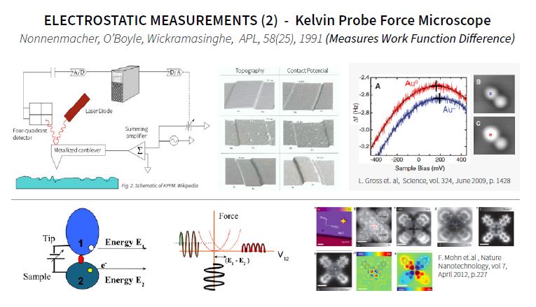
illustrating nanoscale mapping of work function differences through detection of tip–
sample electrostatic interactions.
Optical Nanoscopy and Near-Field Techniques
Beyond mechanical and electrical measurements, scanning probe microscopes also opened new possibilities for optical characterization at spatial resolutions far below the diffraction limit of conventional microscopy.
Near-field optical microscopy achieves this by detecting electromagnetic fields in the immediate vicinity of a sample surface. Early approaches used small apertures at the end of tapered optical fibers to confine light to nanoscale regions. Later developments introduced apertureless near-field optical microscopy, in which a sharp AFM tip acts as a nanoscale antenna that scatters light interacting with the sample surface.
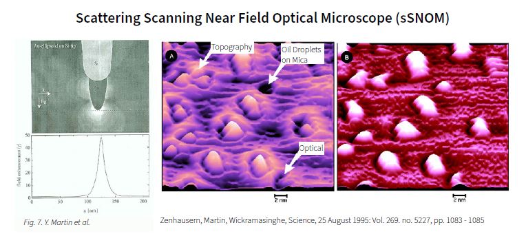
(Top) Localized field enhancement at a metal-coated AFM tip apex enables nanoscale
optical interaction beyond the diffraction limit. (Bottom) Correlated topography and
optical images of oil droplets on mica, demonstrating simultaneous structural and
optical contrast at nanometer-scale resolution.
When illuminated by a focused laser beam, the tip–sample system produces scattered light carrying information about local optical properties. Interferometric detection methods can measure the amplitude and phase of this scattered signal with high sensitivity, enabling optical imaging with nanometer-scale resolution.
These techniques made it possible to study nanoscale optical phenomena such as molecular orientation, plasmonic interactions, and phonon polaritons in advanced materials.
Photo-Induced Force Microscopy
An important extension of optical scanning probe techniques is photo-induced force microscopy (PiFM), which combines AFM with optical spectroscopy. In this method, incident light polarizes both the probe tip and the sample surface. The resulting electromagnetic interaction generates a small force that can be detected by the cantilever.
By measuring this photo-induced force while tuning the wavelength of the incident light, the microscope can obtain nanoscale infrared spectra of materials. This enables chemical identification and molecular characterization with spatial resolutions far beyond the capabilities of conventional optical spectroscopy.
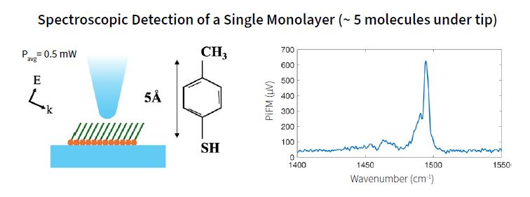
signals originating from only a few molecules beneath the tip.
PiFM has been used to study molecular monolayers, polymer materials, and nanoscale structures in two-dimensional materials. In many cases, the technique allows researchers to detect chemical signatures from extremely small volumes of material, approaching the sensitivity needed for single-molecule spectroscopy.
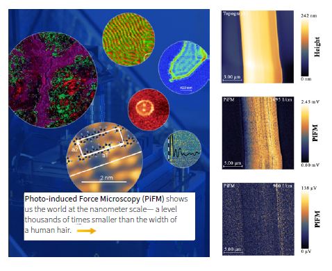
acquired on- and off-resonance, highlighting chemical
contrast enabled by PiFM through selective excitation
of molecular vibrational modes achieving a spatial
resolution independent of the topography.
Toward Multifunctional Nanoscale Measurement
Over the past four decades, AFM has evolved into a multifunctional platform capable of measuring a wide variety of physical properties with nanometer-scale resolution. Modern scanning probe techniques can simultaneously probe surface morphology, electrical potential, magnetic fields, optical responses, and thermal behavior.
This ability to correlate multiple properties at the same location provides powerful insights into nanoscale phenomena. In semiconductor research, it enables detailed characterization of device structures and materials. In materials science, it allows researchers to study the interplay between structure, chemistry, and physical behavior at nanometer length scales.
The continuing evolution of scanning probe microscopy reflects the broader trend in nanoscience toward integrated measurement platforms capable of combining multiple analytical techniques in a single instrument.
Conclusion
Since its introduction in 1986, atomic force microscopy has become one of the most important tools in nanoscale science and technology. Advances in instrumentation, detection methods, and measurement techniques have transformed AFM from a simple surface imaging device into a comprehensive platform for nanoscale characterization.
As highlighted in Prof. Wickramasinghe’s presentation at the Stanford NanoScientific Symposium, the early development of non-contact AFM and the expansion of scanning probe methods into electrical, magnetic, optical, and chemical measurements laid the foundation for today’s multifunctional nanoscopy techniques.
Looking forward, scanning probe microscopy will continue to play a central role in advancing nanoscience, enabling researchers to explore and understand the physical properties of materials with unprecedented spatial resolution.
About Kumar Wickramasinghe
Professor Kumar Wickramasinghe is a pioneering researcher in scanning probe microscopy and nanoscale measurement science. A Distinguished Professor at the University of California, Irvine, he previously conducted influential research at IBM Research, where his group helped advance atomic force microscopy beyond surface imaging to multifunctional nanoscale characterization. His work contributed to the development of techniques such as non-contact AFM, Kelvin probe force microscopy, magnetic force microscopy, and photo-induced force microscopy (PiFM), enabling measurements of electrical, magnetic, optical, and chemical properties at nanometer and molecular scales.
