From Laboratory Curiosity to Industrial Infrastructure: The Commercial Evolution of AFM — A Founder’s Perspective on Building Park Systems and Industrializing Atomic Force Microscopy
- 20 May 2026
- Volume 30
- NANOscientific Magazine, 2026
Dr. Sang-il Park, Founder and CEO, Park Systems Corp., Gwacheon, South Korea
The Dawn of a New Instrument
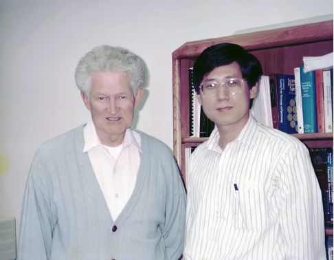
In the early 1980s, as scanning tunneling microscopy (STM) began revealing atomic images of silicon surfaces, a quiet revolution was taking shape at Stanford University. Under the leadership of Calvin Quate, researchers were pushing beyond the limits of optical microscopy and redefining what it meant to “see” matter.
Achieving atomic resolution was not routine—it demanded patience, precision, and sometimes luck. For those who succeeded, it felt like entry into an exclusive club. Yet even at that early stage, it was clear that STM had limitations. It required conductive samples, leaving vast categories of materials beyond reach.
The breakthrough came when the idea that would become atomic force microscopy (AFM) emerged: instead of relying on tunneling current, it utilized the interaction forces between a sharp probe tip and the sample surface. This concept was realized in 1985 and formally introduced in 1986, marking the birth of AFM. This approach enabled imaging of virtually any material—conductive or insulating—at the atomic scale.
The commercialization path that followed would eventually take shape through the founding and growth of Park Systems. But at the time, AFM was still a fragile laboratory apparatus—powerful, but far from industrially ready.
The First Commercialization Wave
In the late 1980s, AFM remained largely confined to research laboratories. Commercializing such an instrument required not only engineering refinement but business conviction.
In 1988, I founded Park Scientific Instruments (PSI) to bring AFM into broader scientific use. In 1990, we introduced the first commercial atomic force microscope, marking the beginning of AFM’s transition from a laboratory instrument to a practical research tool. Early systems brought AFM to universities and research institutes worldwide.
By licensing cantilever technology developed at Stanford University, we also established a reliable probe supply chain—at one point even supplying competitors.
However, early success did not guarantee stability. The early 1990s brought intensified competition from well-funded entrants. Shrinking margins and financing pressures pushed the young company to the brink of collapse. A painful restructuring followed, along with new investment and strategic partnerships that enabled survival and eventual recovery.
Those formative years revealed a central truth about scientific instrumentation: technological brilliance is necessary but insufficient. Commercial viability demands operational discipline, capital management, and long-term resilience.
By the late 1990s, consolidation reshaped the AFM landscape. Companies merged, were acquired, and reorganized. The field was transitioning from pioneering startups into structured industrial players. The AFM industry was maturing.
A Second Beginning: Rebuilding with a New Architecture
After returning to Korea, a second venture began—initially as PSIA, later renamed Park Systems. This phase was not about repeating earlier commercialization efforts, but about rethinking AFM from the ground up.
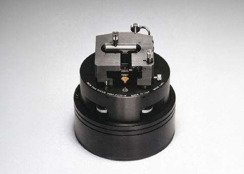
First-generation commercial AFMs had demonstrated market demand, yet they carried fundamental technical limitations. Most relied on tube scanners—a simple solution for nanoscale positioning but prone to cross-coupling between axes. Even flat surfaces could appear distorted.
For research, this was manageable. For metrology, it was unacceptable.
A major architectural shift emerged with the separation of XY and Z scanners, each based on flexure-guided mechanisms and stacked piezo actuators. By fully decoupling lateral and vertical motion—particularly through an independent Z scanner—this orthogonal scan design eliminated cross-talk and enabled true metrology-grade accuracy. Higher resonance frequencies further improved measurement stability and scan speed.
Equally significant was the stabilization of true non-contact mode in ambient conditions. Early systems relied heavily on tapping mode due to the difficulty of maintaining stable non-contact operation. However, tapping introduced tip wear, limiting measurement accuracy and repeatability. By refining scanner mechanics, feedback control, and system stability, it became possible to maintain operation strictly within the attractive force regime. This enabled minimal tip degradation, improving measurement reliability, particularly for high-aspect-ratio structures, soft materials, and advanced semiconductor applications.
Control theory played a central role in advancing AFM performance. By quantitatively modeling the feedback loop, the relationships among scan speed, surface slope, feedback gain, and tracking error could be clearly defined. This enabled systematic optimization of operating conditions, replacing empirical tuning with predictable and reproducible performance.
These advances enabled the transition from manually tuned instruments to increasingly automated systems. Automation was implemented at multiple levels, including probe handling, alignment, and system calibration, forming the foundation for fully automated AFM operation in both research and industrial environments:
- Pre-mounted probe carriers with encoded identification
- Kinematic mounting for repeatable positioning
- Automatic tip exchange modules
- Integrated machine vision for laser alignment
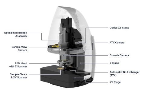
These developments culminated in automated AFM platforms such as the FX series, where users define scan size, resolution, and quality preference, and the system optimizes remaining parameters in real time. AFM was evolving from a skilled-operator instrument into a robust measurement platform.
Crossing the Industrial Threshold
Transitioning AFM from a laboratory instrument to an industrial metrology tool required meeting the stringent demands of semiconductor manufacturing. These include high repeatability, system uptime, full automation, fab integration, and data traceability—requirements far beyond those of typical research environments.
At the same time, continued device scaling and the introduction of complex 3D architectures created measurement challenges beyond the capabilities of conventional optical techniques. Parameters such as line edge roughness, sidewall angles, nanoscale topography, and defect characterization required atomic-scale resolution combined with high measurement accuracy.
To address these requirements, Park Systems industrial AFMs were developed with capabilities tailored for semiconductor process control, including:
- 300 mm wafer handling
- Fully automated navigation
- SECS/GEM communication protocols
- Environmental control
- High-throughput architectures
Joint development programs with leading research institutions such as imec marked critical validation milestones. These collaborations demonstrated AFM’s suitability for advanced node metrology and 3D stacking applications.
Applications expanded across semiconductor manufacturing, covering both front-end and back-end processes:
Front-End
- Surface roughness metrology
- Height, depth, width, and angle measurements
- CMP metrology
- Wafer edge (bevel) metrology
- Defect review
- Electrical conductivity measurements
Back-End
- Copper pad height metrology
- Redistribution layer (RDL) metrology
- DUV/EUV mask defect review
- Defect repair using AFM probes
These capabilities established AFM as a versatile metrology platform across multiple stages of semiconductor manufacturing.
The Rise of Park Systems Within a Consolidating Industry
The AFM industry has undergone multiple consolidation waves. Early pioneers—including Park Scientific Instruments, Digital Instruments, and TopoMetrix—were absorbed into larger metrology groups over time. Companies such as Veeco and later Bruker played significant roles in shaping the competitive landscape.
Within this evolving environment, Park Systems—rebuilt from its second founding—pursued steady expansion through technological differentiation rather than scale alone. Over the past two decades, it has grown into a global AFM manufacturer with installations in research institutions and semiconductor fabs worldwide. Today, Park Systems is widely recognized as the AFM industry leader, with approximately $150 million in annual revenue and a market capitalization exceeding $1 billion.
Public listing in 2015 marked a structural transition from entrepreneurial venture to globally recognized corporation. Strategic acquisitions broadened capabilities into adjacent nanoscale metrology domains, including ellipsometry, vibration isolation, and digital holographic microscopy.
The trajectory reflects not simply corporate growth, but the maturation of AFM as a cornerstone measurement technology.
Beyond Technology: The Human Dimension
Over four decades, AFM’s transformation has also reflected broader lessons in leadership and purpose. Early efforts focused on invention and survival, while later experience underscored the importance of organizational culture—trust, accountability, and long-term commitment. Sustained innovation requires not only technical excellence, but also disciplined execution and clarity of purpose.
At a certain stage, financial success becomes secondary to value creation. When confronted with a major acquisition offer, the defining question was not valuation, but direction: would selling maximize value for society, or would continued innovation create greater long-term impact?
The choice was to continue building.
True entrepreneurship means creating something new and sustaining it responsibly. It requires balance—neither driven by fear nor by greed and a long-term commitment to earning respect.
Forty Years Forward
Forty years later, atomic force microscopy has evolved from a laboratory innovation into a foundational tool for nanoscale science and semiconductor manufacturing.Over the past four decades, continuous innovation has transformed
AFM from a laboratory apparatus into a widely used scientific instrument and a critical metrology tool in semiconductor fabrication. Key technological milestones included the development of flexure-based orthogonal scan systems, reliable true non-contact operation, optimized Z-servo control, automated operation through software such as SmartScan, and fully automated semiconductor process-control AFMs. These advances enabled AFM to move beyond academic laboratories and become an essential technology for nanoscale characterization and industrial metrology.
The evolution of AFM is inseparable from the organizations that advanced it from laboratory innovation to industrial infrastructure. Park Systems represents one sustained effort to industrialize and globalize AFM while maintaining its foundation in scientific rigor and engineering precision. More broadly, AFM’s evolution reflects not only advances in physics, but also engineering discipline, entrepreneurship, and long-term commitment. As device dimensions continue shrinking and advanced packaging expands, nanoscale metrology will face even greater demands, and the next forty years will require the same courage that defined the first.
Dr. Sang-il Park is the founder and CEO of Park Systems and founder and CEO of Park Scientific Instruments. He earned his Ph.D. in Applied Physics from Stanford University, where he worked in the laboratory of Calvin Quate during the early years of scanning probe microscopy. Dr. Park has dedicated his career to advancing nanoscale measurement technologies and building globally competitive instrumentation companies in atomic force microscopy.