Deciphering Electrical Bistability In Nanocomposite Devices Using Electrostatic Force Microscopy
- 19 May 2026
- Volume 30
- NANOscientific Magazine, 2026
Prof. Shashi Paul, De Montfort University, Leicester, United Kingdom
Introduction
The search for new electronic memory technologies remains one of the central challenges in modern electronics. As computing systems demand faster processing speeds, higher data density, and reduced power consumption, researchers continue to explore materials and device architectures capable of storing information in fundamentally different ways.
Among the many emerging approaches, nanocomposite materials consisting of insulating polymers embedded with nanoscale or sub-nanoscale bits (nanoparticles, molecules, nanoclusters, etc) have attracted considerable attention¹. These systems can exhibit electrical bistability, meaning that the device can exist in two stable electrical states corresponding to binary information storage².
Electrical bistability has been widely reported in nanocomposite-based devices over the past two decades³. However, despite the large number of studies, the underlying mechanisms responsible for bistable switching remain widely debated. Different research groups have proposed a range of explanations, including charge trapping, filament formation, and interface effects, often even for identical material systems⁴.
In work spanning more than a decade, Prof. Shashi Paul and collaborators at De Montfort University have investigated the physical origins of electrical bistability in nanocomposite devices²˒⁵. By combining device engineering with electrostatic force microscopy (EFM) measurements, their research provides insight into how internal electric fields generated by stored charges can produce bistable electrical behavior in nanocomposite structures⁶˒⁷.
Bistability and Information Storage
In electronic memory systems/device, bistability refers to the presence of two stable states separated by an energy barrier. A system/device can flip from one state to another when sufficient energy is supplied, but once the transition occurs, the system remains in that state until another external stimulus is applied⁸.
This concept forms the basis of binary memory. A simple physical representation of a bistable system is a particle in a double-well energy landscape. Each well represents a stable state. To move from one well to the other, the particle must overcome an energy barrier.
For memory devices, the stability of these states determines how long information can be stored. Ideally, a memory device should maintain its stored state for extended periods without requiring continuous energy input.
However, many conventional electronic memory technologies suffer from charge leakage or degradation over time, which ultimately limits their retention performance. This limitation has motivated research into new materials and physical mechanisms capable of supporting stable bistable behavior. Prof. Shashi Paul is seeking an immortal memory that should remain for eternity after it is written.
Nanocomposite Materials for Memory Devices
In Prof. Paul’s research, a nanocomposite is defined as an admixture of polymer matrix and nano and sub-nano bits (nano-particles, nano-wires, molecules, nano-clusters, etc).
The polymer serves as an electrically insulating medium. Common examples include polystyrene, polyvinyl alcohol, polyvinyl acetate, polyvinyl phenol. These polymers exhibit low electrical conductivity and can be processed into thin films suitable for electronic devices.
Nanoparticles or molecular species are introduced into the polymer matrix to modify its electrical properties. These inclusions may be metallic, semiconducting, or molecular in nature. Their presence introduces localized sites capable of interacting with charge carriers.
Once fabricated, the nanocomposite film is typically sandwiched between two metal electrodes, forming a simple two-terminal electronic device. By applying a voltage across the electrodes, the resulting current–voltage characteristics can reveal whether bistable switching occurs.
Despite the structural simplicity of such devices, the mechanisms governing their electrical behavior can be surprisingly complex.
Early Studies of Nanocomposite Bistability
Interest in nanocomposite memory devices increased significantly following several experimental demonstrations in the early 2000s. One early example involved the organic compound Alq₃ (tris(8-hydroxyquinolinato)aluminum) and C₆₀ embedded in Polystyrene and sandwiched between metal electrodes³. This study revealed hysteresis in the current–voltage response, suggesting the presence of bistable electrical states.
Another widely cited study incorporated gold nanoparticles blended with polymer materials. When this nanocomposite film was sandwiched between electrodes, the resulting device exhibited clear bistable switching behavior⁶.
Following these pioneering experiments, numerous research groups began exploring nanocomposite memory devices using a wide variety of materials and fabrication approaches. However, the reported electrical characteristics varied widely.
Typical parameters reported in the literature include:
- On/off current ratios ranging from 10 to 10⁹
- Retention times ranging from seconds to several weeks
- Switching endurance ranging from tens to millions of cycles
In addition, the shapes of the current–voltage curves differed considerably, with behaviors often described as N-shaped, S-shaped, or O-shaped switching characteristics⁹. Such variability suggested that the underlying mechanisms were not yet fully understood⁴.
Conflicting Conduction Mechanisms
A major challenge in understanding nanocomposite bistability is the lack of agreement regarding the conduction mechanisms responsible for switching.
Even when identical materials are studied, different research groups often propose different explanations for the observed electrical behavior. These include mechanisms such as:
- Charge trapping within nanoparticles
- Formation of conductive filaments
- Interface-related conduction processes
- Space-charge-limited transport
This lack of consensus motivated Prof. Shashi Paul and his collaborators to revisit the problem from a more fundamental perspective.
Rather than attempting to interpret experimental results using existing models, their approach focused on developing a physical explanation based on first principles, beginning with the role of charge storage and internal electric fields.
Internal Electric Fields as the Origin of Bistability
A key concept emerging from this work is that excess charge within a material inevitably generates an electric field.
Charges can accumulate in several locations within a device: on material surfaces, at defect sites, within embedded nanoparticles. When these charges are present, they create internal electric fields that influence the transport of charge carriers through the device.
A simple physical analogy involves a dipole placed near a charged electrode. Depending on the orientation of the dipole, the potential distribution within the system changes. Reversing the dipole orientation produces a different potential configuration.
If a system can switch between such configurations, it can exhibit two stable electrical states, corresponding to bistability. In nanocomposite materials, nanoparticles can act as charge storage centers. Charges trapped in these nanoparticles create local electric fields that affect current flow through the device.
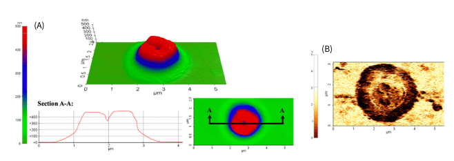
Investigating Charge Storage with Electrostatic Force Microscopy
To experimentally investigate charge storage in nanocomposite systems, the researchers employed electrostatic force microscopy (EFM).
EFM is a scanning probe microscopy technique capable of detecting electrostatic interactions between a probe tip and a sample surface. These interactions arise from local electric fields and surface charges.
By measuring the forces acting on the probe tip, EFM can map charge distributions across a surface with nanoscale spatial resolution.
The experiments were performed using a Park Systems XE-100 scanning probe microscope, which provides multiple imaging modes suitable for nanoscale electrical characterization.
The device structures studied consisted of:
- A silicon substrate
- A silicon dioxide insulating layer
- Metal electrodes
- A nanocomposite film containing nanoparticles and also just nanoparticles
Using the AFM probe tip, charges could be locally injected into the nanocomposite/nanoparticles surface. Subsequent EFM imaging allowed the researchers to observe how these charges evolved over time.
Charge Retention in Nanocomposite Systems
Initial experiments focused on determining how long stored charges remain in the nanocomposite material. EFM images revealed bright regions corresponding to localized surface charge. By repeatedly imaging the same area, the researchers observed that these charges gradually dissipated over time. In many cases, the stored charge decayed within approximately one hour.
Control experiments were also performed using pure polymer films without nanoparticles. These experiments showed that polymers themselves can also store charge temporarily, although the charge typically dissipates relatively quickly.
This finding emphasized the importance of carefully distinguishing between the roles of the polymer matrix and the embedded nanoparticles when interpreting bistability measurements.
Direct Charging of Individual Nanoparticles
To better understand charge storage at the nanoscale, the researchers conducted experiments in which individual nanoparticles were charged using the AFM probe tip. In one experiment, a collection of nanoparticles was deposited onto an electrode surface. Most of the nanoparticles formed conductive pathways connected to the electrode, but a few particles remained electrically isolated.
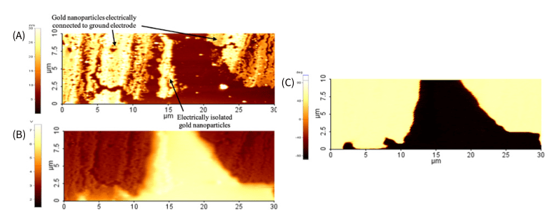
These measurements provided direct evidence that nanoparticles can temporarily store electrical charge, supporting the hypothesis that charge accumulation plays an important role in nanocomposite bistability.
Filament Formation and Device Variability
In some nanocomposite devices, extremely large on/off current ratios have been reported. These large switching ratios are often attributed to the formation of conductive filaments within the device.

However, atomic force microscopy imaging revealed that such filament formation often leads to high device-to-device variability. From a device engineering perspective, this variability is undesirable. Reliable memory devices must exhibit consistent switching behavior across large arrays of devices.
Therefore, while filament formation can produce large switching currents, it may represent device failure rather than a reliable switching mechanism.
A Simple Physical Model
Based on their experimental findings, the researchers proposed a simple model to explain electrical bistability in nanocomposite systems.
The model suggests that bistability occurs when:
- Charge carriers become trapped in nanoparticles.
- These charges generate an internal electric field.
- The internal electric field alters the effective electric field across the device.
As a result, the device exhibits two different current levels when measured under identical external voltage conditions. These two current states correspond to the bistable states of the memory device. The retention time of the device depends on how long the stored charge—and therefore the internal electric field—can be maintained.
Conclusion
Electrical bistability in nanocomposite materials has been widely observed but remains poorly understood. Through a systematic investigation combining device fabrication and electrostatic force microscopy, Prof. Shashi Paul and collaborators have provided important insights into the physical mechanisms underlying this phenomenon.
Their work demonstrates that bistable behavior can arise from internal electric fields generated by charges stored in nanoparticles embedded within polymer matrices. Electrostatic force microscopy provides a powerful tool for directly visualizing these charge distributions and understanding their temporal stability.
Ultimately, the stability of the internal electric field determines how long information can be retained in such devices. By carefully controlling charge storage and nanoparticle distribution within nanocomposites, it may be possible to design new classes of electronic memory devices with improved efficiency and stability.
These findings highlight the importance of combining nanoscale characterization techniques with device-level analysis to fully understand the behavior of emerging electronic materials.

Shashi Paul (SP), Professor of Nanoscience and Nanotechnology, works at the Emerging Technologies Research Centre (EMTERC) at De Montfort University, Leicester, UK. He received his degree from the Indian Institute of Science, Bangalore, India, and previously worked at the University of Cambridge, Durham University, and Rutgers University. His particular focus is on emerging electronic memory devices, batteries and solar cells, and the development of materials manufacturing processes to reduce the carbon footprint of next-generation electronic devices.
Since his teenage years, he has regarded research and teaching as a passion rather than a profession. He believes that teaching and research are like binary stars—they either exist or they do not—and that an invisible force, which cannot be seen but can be felt, is the foundation of their existence. Playing and watching cricket is also something he thoroughly enjoys.
References
- Shashi Paul, “Organic and Macromolecular Memory – Nanocomposite Bistable Memory Devices,” in Advances in Semiconductor Technologies: Selected Topics Beyond Conventional CMOS, First Edition. Edited by An Chen. © 2023 The Institute of Electrical and Electronics Engineers, Inc. Published 2023 by John Wiley & Sons, Inc.
- F. Paul and S. Paul, “Electrical Bistability by Creating an Internal Electrical Field and Its Application in Emerging Two-terminal Electronic Memory Devices,” in Advanced Memory Technology, Royal Society of Chemistry, 2023, pp. 149–182. doi: 10.1039/BK9781839169946-00149.
- S. Paul, “Realization of nonvolatile memory devices using small organic molecules and polymer,” IEEE Trans. Nanotechnol., vol. 6, no. 2, 2007, doi: 10.1109/TNANO.2007.891824.
- F. Paul and S. Paul, “To Be or Not to Be – Review of Electrical Bistability Mechanisms in Polymer Memory Devices,” Small, vol. 18, no. 21, May 2022, doi: 10.1002/smll.202106442.
- F. Paul, K. Nama Manjunatha, and S. Paul, “Non-Zero and Open-Loop Current–Voltage Characteristics in Electronic Memory Devices,” Adv. Electron. Mater., vol. 9, no. 10, 2023, doi: 10.1002/aelm.202300324.
- D. Prime, S. Paul, and P. W. Josephs-Franks, “Gold nanoparticle charge trapping and relation to organic polymer memory devices,” Philosophical Transactions of the Royal Society A: Mathematical, Physical and Engineering Sciences, vol. 367, no. 1905, 2009, doi: 10.1098/rsta.2009.0141.
- D. Prime and S. Paul, “First contact-charging of gold nanoparticles by electrostatic force microscopy,” Appl. Phys. Lett., vol. 96, no. 4, 2010, doi: 10.1063/1.3300731.
- S. Paul, Organic and macromolecular memory - nanocomposite bistable memory devices. 2022.
- D. Prime and S. Paul, “Overview of organic memory devices,” Philosophical Transactions of the Royal Society A: Mathematical, Physical and Engineering Sciences, vol. 367, no. 1905, 2009, doi: 10.1098/rsta.2009.0165.