Charge-Transfer Polaritons in Van Der Waals Heterojunctions: Unlocking New Frontiers In Graphene Plasmonics
- 10 Nov 2025
- Volume 29
- NANOscientific Magazine, 2025
Prof. Brian Kim, University of Arizona
Adapted from Presentation, Edited by NanoScientific
Introduction: Expanding the Design Space of 2D Polaritons
At the 2024 NanoScientific Symposium, Prof. Brian Kim from the University of Arizona introduced a major step forward in nanophotonics—the creation of highly tunable charge-transfer polaritons in van der Waals (vdW) heterojunctions. His work demonstrates how precisely engineered oxide–graphene interfaces can generate stable, low-loss graphene plasmons with exceptional lateral doping resolution, all without the drawbacks of traditional gating or lithography.
Polaritons—quasiparticles formed from the strong coupling of light and matter—are a foundation for advanced optical and quantum devices. In graphene, surface plasmon polaritons (SPPs) combine extraordinary confinement (more than 100× shorter wavelength than light in vacuum) with low intrinsic loss, tunability, and compatibility with layered materials. However, their implementation has been hindered by a practical challenge: how to introduce large carrier densities into graphene with nanometer precision, without physically degrading the lattice or blurring the doping profile.
Prof. Kim’s solution uses a subtle but powerful physical effect—work function mismatch at engineered oxide interfaces—to “write” doping patterns directly into pristine graphene.
Polaritons in 2D Materials: Why Graphene Is Special
In polaritonic systems, electromagnetic waves couple strongly with excitations such as plasmons (collective oscillations of electrons) or phonons (lattice vibrations). At the interface between two materials with opposite signs of dielectric function, these hybrid modes can propagate along the boundary.
Graphene is an ideal host for polaritons because:
• SPPs exist only at high doping levels, enabling tunable activation by carrier density.
• Plasmonic modes in graphene are low-loss due to Pauli blocking of electron–hole scattering, unlike metals where damping from conduction electrons is unavoidable.
• Its vdW nature allows precise stacking with other 2D materials to hybridize modes and engineer novel dispersion relations.
Moreover, graphene’s plasmons produce strong confinement and enable manipulation of optical modes deep below the diffraction limit—over a broadband from THz into the mid-infrared regime.
The Challenge: Patterning Graphene Plasmonic Cavities Without Detriment
To take advantage of these properties, one must be able to create nanoscale patterns of high carrier density to realize plasmonic cavities or photonic crystals while preserving the exceptional mobility and crystalline perfection of graphene.
Traditional strategies—such as directly etching graphene into nanostructures or patterning local gates beneath it—come with serious drawbacks. Etching produces rough edges that scatter plasmons. Patterned gates limit flexibility, introduce dielectric inhomogeneities, and require close spacing that constrains optical mode design. Both approaches blur the lateral doping profile, reducing mode sharpness and cavity Q factors.
Prof. Kim’s group sought an alternative that could:
• Avoid physical damage to the graphene lattice.
• Precisely control doping strength and profile shape.
• Eliminate the need for patterned gates.
Work Function Mismatch: Gate-Free Ambipolar Doping
The breakthrough comes from harnessing electrostatics. When two materials with different work functions are brought into intimate contact, charge-transfers across the interface until the Fermi levels align.
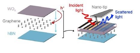
Prof. Kim’s team transfers atomically thin layers of high–work function transition metal oxides on graphene. In their work, tungsten oxide (WOx) is created in situ by oxidizing tungsten diselenide (WSe2) layers using ultraviolet ozone treatment. Crucially, this oxidation is self-limiting: only the outermost monolayer of WSe2 converts to WOx, while the underlying structure remains intact.
This approach offers several advantages:
• No etching or gate electrodes are required.
• The oxide induces substantial, uniform hole doping through work function mismatch.
• Lateral doping boundaries are atomically sharp.
By designing vdW heterostructures where a high-work-function WOx sits atop monolayer graphene encapsulated in hexagonal boron nitride (hBN), the group achieves extremely high hole densities (on the order of 4×10¹³ cm⁻²) without external gating. By substituting WOx with low–work function zirconium oxide (ZrOx), Prof. Kim’s group achieves electron doping of graphene to similarly high densities, confirming the robustness of the charge-transfer technique. This ambipolar charge-transfer doping significantly expands access to optical properties and transport regimes in vdW heterostructures previously unreachable with conventional electrostatics.
Probing the Charge-Transfer Plasmons via s-SNOM Imaging
To verify charge-transfer and map plasmon propagation, the team employs scattering-type scanning near-field optical microscopy (s-SNOM)—a technique that combines atomic force microscopy with infrared illumination at the nanoscale.
In Prof. Kim’s images, distinct plasmonic interference fringes appear along the oxide–graphene interface. These standing wave patterns are formed by plasmons launched from the s-SNOM tip, reflected at conductivity boundaries, and interfered on their return. The visibility and uniformity of these fringes confirm both effective doping and high material quality. Fitting the fringe decay to a damped oscillator model yields a plasmon quality factor Q of ~16, already approaching the performance of silver films at comparable frequencies.
Because the oxidation process affects only the exposed surface, the team can control charge-transfer with atomic precision by inserting layers of unoxidized WSe2 as spacers between WOx and graphene. Each monolayer acts as a nanometer-scale buffer, modulating the effective work function mismatch and thus the doping level. Increasing the spacer thickness reduces the plasmon wavelength (corresponding to reduced carrier density) while improving Q due to diminished scattering from charged impurities in the oxide. Remarkably, a single bilayer spacer (~7 Å thick) reduces scattering enough to raise Q to ~30—surpassing noble metals and approaching the intrinsic phonon-limited behavior of graphene plasmons at room temperature.
oxide–graphene interfaces imaged via s-SNOM technique.
Creating Plasmonic Nanocavities Without Physical Etching
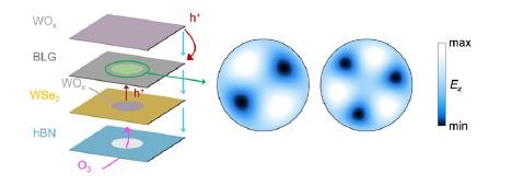
This charge-transfer approach enables a powerful fabrication strategy: mask-defined plasmonic cavities in continuous graphene. By placing a pre-patterned hBN mask with nanoscale apertures over graphene before oxidation, Prof. Kim’s team can locally expose regions to WOx formation. The result is a pattern of high-density, plasmon-active regions embedded in a continuous sheet of pristine graphene.
s-SNOM imaging confirms strong cavity modes within these regions. Finite-element simulations show that lateral doping transitions sharper than ~6 nm are achieved using this method, yielding well-confined modes without lattice disruption.
The group further demonstrates suspended graphene plasmonic cavities that can be doped from both the top and bottom via WOx. Dispersion mapping verifies hole-doping, showing that doping density increased by ~30%. Importantly, these suspended cavities support whispering gallery modes, plasmon waves circulating along the cavity perimeter, forming standing wave patterns governed by cavity size and excitation frequency. These modes, observed here in graphene for the first time, demonstrate the potential for control over strong light–matter interactions in engineered 2D cavities.
gallery cavities based on suspended oxide–graphene heterostructures.
A New Platform for Graphene Plasmonic Nanocavities
Prof. Kim’s team demonstrates how the charge-transfer graphene plasmonic nanocavities described above can open up new research directions in controlling polaritons.
As one example, the group shows that charge-transfer graphene plasmonic cavities can strongly hybridize with phonon polaritons in proximal 2D materials, such as molybdenum oxide (α-MoO₃) that supports hyperbolic phonon polaritons with open, directional iso-frequency contours. In particular,
Placing graphene plasmonic cavities atop α-MoO₃ induces a topological transition in the iso-frequency contour from an open hyperbola into a closed oval-shaped contour. This fundamentally modifies the polariton topology, opening new pathways for controlling polariton flow in integrated nanophotonic circuits.
In a final experimental direction, the group explores strain-engineered plasmonics. Non-uniform strain gradients in suspended graphene can generate pseudomagnetic fields mimicking Landau quantization without external magnets. In hexagonal suspended WOx–graphene plasmonic cavities actuated by local back gates, Prof. Kim’s team observes suppression of bulk plasmon response with residual edge-localized modes—consistent with Landau level formation. These features suggest the opening of topologically nontrivial plasmonic gaps.
Conclusion: A New Fabrication Paradigm for 2D Polaritons
Prof. Brian Kim’s work represents a paradigm shift in the fabrication and control of polaritons in graphene and vdW heterostructures. By using work-function mismatch and self-limited oxidation to create nanometer-precise ambipolar doping patterns, his team has removed the reliance on gates and etching—longstanding obstacles in 2D plasmonics.
The ability to write, tune, and couple high-Q plasmonic cavities directly into pristine graphene opens new frontiers:
• Tunable infrared photonics without lossy gating structures.
• Hybrid polaritons with engineered dispersion in vdW stacks.
• Topologically robust modes via strain and dual-surface doping.
Prof. Kim’s research demonstrates that subtle electrostatics, carefully applied, can redefine what is possible in 2D polaritonics—ushering in a new era of precision-engineered nanophotonics and nanoplasmonics.

Dr. Brian S. Y. Kim is an Assistant Professor of Materials Science
& Engineering and Physics at the University of Arizona. He
earned his Ph.D. in Electrical Engineering from Stanford
University and completed postdoctoral research at Columbia
University, specializing in two-dimensional quantum materials
and heterostructures. His research focuses on engineering
atomically precise quantum systems for advanced electronic,
photonic, and quantum technologies, using tools like nanooptical
imaging and reconfigurable device architectures. In
2024, he received the Outstanding Young Researcher Award
from the Association of Korean Physicists in America and the
Korean Physical Society. In 2025, he was named to the Early
Career Editorial Advisory Board of APL Photonics and selected
as Scialog Fellow in Quantum Matter and Information by
Research Corporation for Science Advancement.
References
-
Choi, M. S., Nipane, A., Kim, B. S. Y., Ziffer, M. E., Datta, I., Borah, A., Jung, Y., Kim, B., Rhodes, D., Jindal, A., Lamport, Z. A., Lee, M., Zangiabadi, A., Nair, M. N., Taniguchi, T., Watanabe, K., Kymissis, I., Pasupathy, A. N., Lipson, M., Zhu, X., Yoo, W. J., Hone, J. & Teherani, J. T. High carrier mobility in graphene doped using a monolayer of tungsten oxyselenide. Nature Electronics, 4, 731 (2021).
-
Kim, B. S. Y., Sternbach, A. J., Choi, M. S., Sun, Z., Ruta, F. L., Shao, Y., McLeod, A. S., Xiong, L., Dong, Y., Chung, T. S., Rajendran, A., Liu, S., Nipane, A., Chae, S. H., Zangiabadi, A., Xu, X., Millis, A. J., Schuck, P. J., Dean, C. R., Hone, J. C. & Basov, D. N. Ambipolar charge-transfer graphene plasmonic cavities. Nature Materials, 22, 838 (2023).
-
Ruta, F. L., Kim, B. S. Y., Sun, Z., Rizzo, D. J., McLeod, A. S., Rajendran, A., Liu, S., Millis, A. J., Hone, J. C. & Basov, D. N. Surface plasmons induce topological transition in graphene/α-MoO₃ heterostructures. Nature Communications, 13, 3719 (2022).
Category