Atomic Force Microscope (AFM)-Based Nanomanufacturing Assisted by Vibration and Heat
- 03 Jan 2020
- Volume 18
- NanoScientific Magazine, Winter 2020
Jia Deng, Asst. Professor, Dept. of Systems Science and Industrial Engineering at Binghamton University
Selected Publications:
• X. Kong, J. Deng, J. Dong, and P. H. Cohen, “Study of Tip Wear for AFM-based Vibration-Assisted Nanomachining Process,” J. Manuf. Process. (Accepted)
• H. Zhou, C. Dmuchowski, C. Ke, and J. Deng*. “External-Energy-Assisted Nanomachining with LowStiffness AFM Probe,” Manufacturing Letters, vol. 23, pp. 1–4, Jan. 2020.
• L. Mei, G. Wang, J. Deng, J. Xiao, and X. Guo, “Tunable fabrication of concave microlens arrays by initiative cooling based water droplets condensation,” Soft Matter, 15, pp. 9150-9156, Oct. 2019.
• J. Deng, H. Zhou, J. Dong, and P. Cohen. “ThreeDimensional Nanomolds Fabrication for Nanoimprint Lithography,” Procedia Manuf.,2019
• J. Deng, J. Dong, and P. Cohen. “Rapid Fabrication and Characterization of SERS Substrates,” Procedia Manuf., vol. 26, pp. 580-586, Aug. 2018.
• J. Deng, J. Dong and P. H. Cohen, "Development and Characterization of Ultrasonic Vibration Assisted Nanomachining Process for Three-Dimensional Nanofabrication," IEEE Trans. Nanotechnol., vol. 17, no. 3, pp. 559-566, May 2018.
• G. Wang, J. Deng, and X. Guo, “Electrohydrodynamic assisted droplet alignment for lens fabrication by droplet evaporation,” J. Appl. Phys., vol. 123, no. 16, p. 163102, Apr. 2018.
• J. Deng, L. Zhang, J. Dong, and P. H. Cohen, “AFMbased 3D nanofabrication using ultrasonic vibration assisted nanomachining,” J. Manuf. Process., vol. 24, Part 1, pp. 195–202, Oct. 2016.
• J. Deng, J. Dong, and P. Cohen, “High Rate 3D Nanofabrication by AFM-based Ultrasonic Vibration Assisted Nanomachining,” Procedia Manuf., vol. 5, pp. 1283–1294, Jan. 2016.
Introduction
Maskless nanolithography techniques are critical to fabricate masks and molds for mass production, low volume nanodevices, and various research areas. Atomic force microscope (AFM)-based nanomanufacturing, as an emerging low-cost and easy-to-setup maskless nanomanufacturing technique, enables comparable resolution to that of electron beam lithography, which is commonly used for fabricating masks for photolithography and arbitrary nanopatterns.
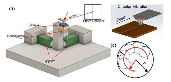
Figure 1. (a) Schematic illustration of the experimental setup for AFM-based nanomanufacturing assisted by vibration and heat. (b) Mechanism of fabricating nanopatterns with controlled width. (C) Schematic illustration of actual feature width, which comprises the vibrational amplitude and the tip diameter.
Different AFM-based nanomanufacturing approaches, such as mechanical direct scratching[1], dynamic plowing[2], thermal-mechanical material removing[3], electrostatic nanolithography[4], and dip-pen nanolithography[5], have been developed as advanced tipbased nanomanufacturing techniques. However, for most existing material removal approaches, the dimensions of nanopatterns are defined by the tip size, which limits the nanomanufacturing capabilities and efficiency. Moreover, relatively large forces are often associated with material removal processes. For example, mechanical scratching commonly requires micro-Newton levelnormal forces to modify surfaces, which leads to quick tip wear and degraded pattern fidelity[6]. Thermal-mechanical technique often needs special thermal probes to implement the technique, although with lower normal force in the range of a few hundreds of nano-Newtons[3]. To easily control the dimensions of nanopatterns and reduce the normal forces, we integrated mechanical vibration and sample heating in the AFM-based nanomanufacturing process[7]. With mechanical vibration, dimensions of nanopatterns can be controlled. The elevated temperature enables a nanomanufacturing process using only tens of nano-Newtons normal forces. Results demonstrated the functions of mechanical vibration and sample heating on enhancing the AFM-based nanomanufacturing capabilities and performances.
Experimental Setup
The experimental setup includes a commercially available AFM from Park Systems (XE-7) amd an in-house fabricated nanomanufacturing stage that integrates the mechanical vibration and thermal energy into the nanomachining process, as shown in Figure 1(a). Two perpendicularly placed piezoelectric actuators generate circular vibration on the sample through the center pillar when the driving sinusoid signals for them have the same amplitude, but 90-degree phase difference. Figure 1(b) illustrates that the circular sample vibration controllably defines the actual dimensions of nanopatterns by simply changing the vibrational amplitude. Figure 1(c) shows the virtual tool radius R, which is the sum of the tip radius r’ and the vibrational amplitude r. AFM tips used for nanomanufacturing were DLC190 and CSG10/Au. In addition to the vibration, the heating element generates the thermal energy on samples. AFM tips canpenetrate through the sample surface easier under elevated temperature than that of no heating because the sample we use in this nanomanufacturing scenario is a thermoplastic material polymethyl methacrylate (PMMA). The sample temperature is positively related to the DC voltage applied to the heating element, and the specific values were calibrated using a thermometer.
For the manufacturing process, vectors and bitmap images can be designed and fabricated on PMMA surfaces by utilizing the lithography software. Forces or height information can be assigned to the vectors and bitmap images to fabricate two dimensional and three dimensional nanopatterns with this experimental setup.
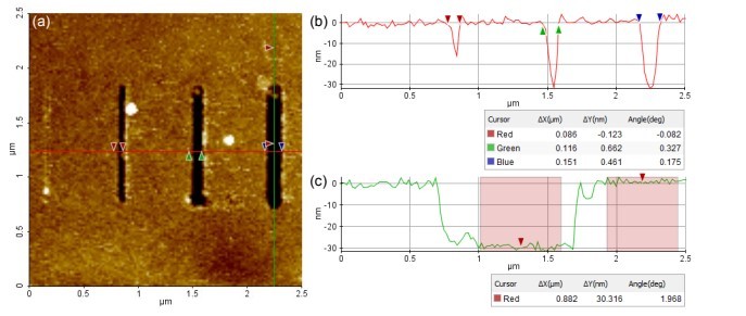
Figure 2: (a) 2D nanopatterns fabricated by employing the in-plane vibration. (b) Cross-sectional profile of all nanopatterns. (C) Cross-sectional profile of the last nanotrench.
Results and Discussions
2D and 3D nanopatterns can be controllably fabricated using the aforementioned AFM-based nanomanufacturing setup[8], [9]. Figure 2 demonstrated that in-plane vibration can effectively tune the dimension of nanopatterns by setting different vibrational amplitude without the limitation of the tip size. Nanopatterns with different widths, 86 nm, 116 nm, and 151 nm in this case, can be fabricated by one single path, which enhances the nanomanufacturing efficiency and capability. In addition to 2D nanopatterns, 3D shapes can also be fabricated. Figure 3shows the grayscale bitmap template image and 3D results on PMMA[10]. The results showed that the nanomanufacturing capability of fabricating arbitrary 3D nanopatterns by the vibration-assisted AFM-based nanomanufacturing. Sample heating was utilized to further decrease the normal force needed for fabricating patterns so as to decrease the tip wear. When the sample surface is slightly heated up to 42°C, a very small normal force of 50 nN can generate nanopatterns, as shown in Figure 4. The tip used for the nanopatterning was very soft CSG10/Au with the nominal spring constant of 0.11 N/m, which is very difficult, if not impossible at all, for nanopatterning in other tip-based nanomanufacturing techniques. The widths and depths of the fabricated nanotrenches are about 45 nm and 8 nm, respectively. We demonstrated that nanopatterns with high fidelity can be fabricated by our proposed AFM-based nanomanufacturing assisted by both vibration and heat.
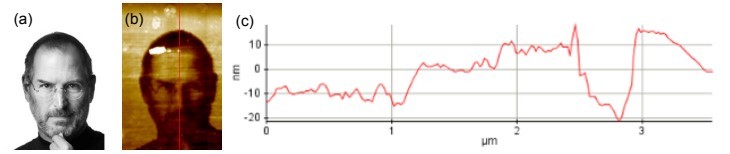
Figure 3: (a) Grayscale bitmap template image of Steve Jobs [11]. (b) 3D nanopatterns fabricated the AFM based nanomanufacturing process [10]. (c) Cross-sectional profile of the result.
Summary
Vibration and thermal energy assisted AFM-based nanomanufacturing can be used to fabricate two dimensional and arbitrary three dimensional nanopatterns for numerous applications. The in-plane vibration provides tunable feature dimensions and higher nanopatterning efficiency. The required normal forces for the nanomanufacturing are reduced to the level of tens of nano-Newtons because the thermal energy applied on the thermoplastic sample softens the sample. Integration of the vibration and heat in the AFM-based nanomanufacturing process enhances the nanopatterning capabilities and performances.
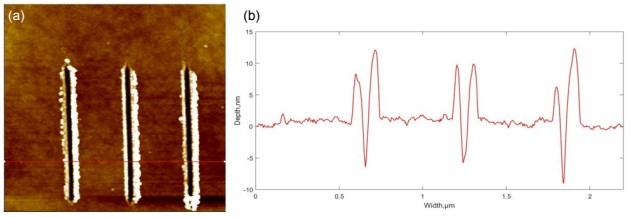
Figure 4: (a) Topography and (b) cross-sectional profile of nanotrenches fabricated by AFM-based nanomanufacturing assisted by vibration and heat using a soft tip CSG10/Au, of which the nominal spring constant is 0.11 N/m.
References
[1] R. Rank, H. Brückl, J. Kretz, I. Mönch, and G. Reiss, “Nanoscale modification of conducting lines with a scanning force microscope,” Vacuum, vol. 48, no. 5, pp. 467–472, May 1997.
[2] B. Klehn and U. Kunze, “Nanolithography with an atomic force microscope by means of vector-scan controlled dynamic plowing,” Journal of Applied Physics, vol. 85, no. 7, pp. 3897–3903, Mar. 1999.
[3] D. Pires et al., “Nanoscale Three-Dimensional Patterning of Molecular Resists by Scanning Probes,” Science, vol. 328, no. 5979, pp. 732–735, May 2010.
[4] M. Ishibashi, S. Heike, H. Kajiyama, Y. Wada, and T. Hashizume, “Characteristics of scanning-probe lithography with a currentcontrolled exposure system,” Appl. Phys. Lett., vol. 72, no. 13, pp. 1581–1583, Mar. 1998.
[5] D. S. Ginger, H. Zhang, and C. A. Mirkin, “The Evolution of DipPen Nanolithography,” Angewandte Chemie International Edition, vol. 43, no. 1, pp. 30–45, Jan. 2004.
[6] Y. Q. Geng et al., “Fabrication of millimeter scale nanochannels using the AFM tip-based nanomachining method,” Applied Surface Science, vol. 266, pp. 386–394, Feb. 2013.
[7] H. Zhou, C. Dmuchowski, C. Ke, and J. Deng, “External-energyassisted nanomachining with low-stiffness atomic force microscopy probes,” Manufacturing Letters, vol. 23, pp. 1–4, Jan. 2020.
[8] J. Deng, L. Zhang, J. Dong, and P. H. Cohen, “AFM-based 3D nanofabrication using ultrasonic vibration assisted nanomachining,” Journal of Manufacturing Processes, vol. 24, pp. 195–202, Oct. 2016.
[9] J. Deng, J. Dong, and P. H. Cohen, “Development and Characterization of Ultrasonic Vibration Assisted Nanomachining Process for Three-Dimensional Nanofabrication,” IEEE Transactions on Nanotechnology, vol. 17, no. 3, pp. 559–566, May 2018.
[10] J. Deng, J. Dong, and P. Cohen, “High Rate 3D Nanofabrication by AFM-based Ultrasonic Vibration Assisted Nanomachining,” Procedia Manufacturing, vol. 5, pp. 1283–1294, Jan. 2016.
[11] W. Isaacson, Steve Jobs. New York; Toronto: Simon & Schuster, 2011.
