Imec Reports in-line 3D AFM Provides Solutions for Semiconductor Manufacturers
- 30 May 2017
- Volume 10
- NanoScientific Magazine, Summer 2017
Imec Is The World-Leading R&D And Innovation Hub In Nanoelectronics
And Digital Technologies Bringing Together Brilliant Minds From All
Over The World In A Creative And Stimulating Environment Accelerating
Progress Towards A Connected, Sustainable Future.
senior researcher at in-line inspection and metrology group imec Belgium
"THE PARTNERSHIP BETWEEN PARK SYSTEMS AND IMEC PROVIDES A CRUCIAL LINK OF SCIENTIFIC COLLABORATION THROUGHOUT THE CHAIN OF SUPPLIERS AND VENDORS IN SEMICONDUCTOR WAFER PRODUCTION CREATING SIGNIFICANT TECHNOLOGICAL ADVANCES IN AFM-BASED INLINE NANOSCALE METROLOGY." DR. SANG-IL PARK, CEO OF PARK SYSTEMS
IMEC PERFORMS WORLD-LEADING RESEARCH IN NANO-ELECTRONICS AND CREATE GROUNDBREAKING INNOVATION IN APPLICATION DOMAINS SUCH AS HEALTHCARE, SMART CITIES AND MOBILITY, LOGISTICS AND MANUFACTURING, AND ENERGY
ABOUT IMEC
Imec is the world-leading research and innovation hub in nanoelectronics and digital technologies. The combination of their widely acclaimed leadership in microchip technology and profound software and ICT expertise is what makes them unique. By leveraging their world-class infrastructure and local and global ecosystem of partners across a multitude of industries, they create groundbreaking innovation in application domains such as healthcare, smart cities and mobility, logistics and manufacturing, and energy. As a trusted partner for companies, start-ups and universities they bring together close to 3,500 brilliant minds from over 70 nationalities. Imec is headquartered in Leuven, Belgium and also has distributed R&D groups at a number of Flemish universities, in the Netherlands, Taiwan, USA, China, and offices in India and Japan.
In 2015, Park systems signed a Joint Development Project (JDP) with imec, to develop in-line AFM metrology solutions of future technology nodes including but not limited to surface roughness, thickness, critical dimension (CD), and sidewall roughness. Together, Park and imec are exploring new frontiers of high resolution 3D AFM metrology to address accurate CD, line width roughness (LWR), line edge roughness (LER) measurements, and sidewall roughness during etch, EPI, film deposition, and lithography processes. The imec and Park Systems partnership is developing new in-line monitoring and analysis methods for semiconductor manufacturers as well as new production protocol for better process development and control, which will result in improved device performance and production yield. The high resolution sidewall information on vertical planar and cylindrical structure by Park's new 3D AFM is having a huge impact on the performance of vertical devices such as FinFET, TFET, STT-MRAM and others.
Please describe your background and the work you do at imec.
I studied material science and engineering and got a degree on surface preparation and modification in semiconductor. For topic, studying surface interaction between two species is a key topic to understand mechanism of contamination and removal. As semiconductor device scale is getting decrease industry requires small contaminants removal efficiently without minimize material loss and pattern damage. It requires me to measure particle removal force and pattern collapse force in quantitively. For quantification of those force, particle adhesion and removal forces and pattern collapse force AFM is the only technique to provide the capability and it asked me to study and use AFM since 1999.
How does imec work with Park Systems?
There are two ways of collaborations. Imec explores highly advanced semiconductor devices and use Park NX3DM at different device architectures to find a suitable solution for their process development and its monitoring. In order to find a best solution, imec and Park Systems develop the software and hardware together. We show the results to the imec partner. Second collaboration would be promoting the application results by publication and presentation at various conferences. For on-time result delivery an engineer from Park Systems works at imec to support all in-line AFM activities.
How is in-line (3D) AFM a solution provider for semiconductor manufacturing processing?
Actually, I see many potential AFM applications in semiconductor manufacturing process. Many people doubt about AFM capabilities in semiconductor process due to their slow measurement speed and low throughput. Although the speed could not faster than other optic and electron based metrology technique, the value of result is greater than that of other metrology solutions surprisingly. Primary advantage of AFM in semiconductor is true atomic resolution topography measurement without sample damage which other metrology technique cannot. I just start to show some results at conference and the capability of AFM is promising. We are also working on improving the throughput and it should meet industry needs soon. My main role is bridging the semiconductor industry and AFM industry. One of my common questions is why more than 30 year old AFM technique was not used for semiconductor manufacturing. I found a possible answer while working with Park Systems. One of biggest jobs is explaining semiconductor needs for AFM specialist by finding problems in semiconductor manufacturing in order to prove suitable metrology solutions for semiconductor engineers. There is a need for a paradigm shift and we are actively doing so.
What features of Park AFM are most useful in semiconductor processing?
I truly emphasize that true non-contact measurement provides a strong advantage on atomic resolution and accuracy with no sample damage. Many imec integration engineers were very surprised at the capability of the Park AFM tool because they never saw such nice information and quality before. They rely on the measurement more and more because of the capabilities. Actually many people do not believe the advantage of non-contact measurement before the tool installation but afterwards they believe it. Long probe lifetime, which is result of non-contact measurement, is significant advantage in use of process monitoring. I think that Park AFM could only handle high density carbon (HDC) probe with 100 nm length and 10 nm diameter for more than 1000 die measurements. It is more than 2000 imaging using single probe.
What are the latest trends advancing semiconductor wafer production currently?
The latest trend in semiconductor wafers is more and more complex and taller and taller. Device scaling will meet the limit, but the functionality of device increase so the semiconductor device processing trend will go the direction. Many other different materials will be introduced, but it might take a while to study them.
How do you see semiconductor manufacturing changing in the future?
Well. I am not in the position to give a comment, but according to imec manufacturing environment and discussion with partner companies, machine learning and AI based on fab data might be a trend to improve manufacturing quality and efficiency.
“IMEC EXPLORES HIGHLY ADVANCED SEMICONDUCTOR DEVICES AND USE PARK NX3DM AT DIFFERENT DEVICE ARCHITECTURES TO FIND A SUITABLE SOLUTION FOR THEIR PROCESS DEVELOPMENT AND ITS MONITORING. IN ORDER TO FIND A BEST SOLUTION, IMEC AND PARK SYSTEMS DEVELOP THE SOFTWARE AND HARDWARE TOGETHER.”
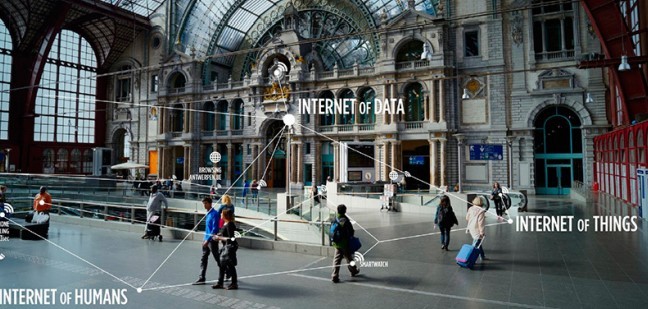
IMEC TRANSFORMS BELGIUM’S CITY OF ANTWERP INTO LIVING LAB FOR THE INTERNET OF THINGS
In this new smart city, businesses, researchers, and local residents, will experiment with smart technologies that aim to make urban life more pleasant, enjoyable, and sustainable. Hundreds of smart sensors and wireless gateways positioned at carefully selected locations across streets and buildings will transform the city into a true living lab for the Internet of Things (IoT). The long-term objective is to connect thousands of Antwerp citizens with numerous innovative solutions that will considerably improve their quality of life – by positively impacting mobility and public safety in the city, among other things.
The essence of a smart city is not that it is crammed full of new technology. First and foremost it is a city in which the quality of l iving is lifted to a new level, fulfilling the practical needs and expectations of the people who live there. To see how this could be realized the city council of Antwerp and a number of committed companies have set up a smart city project, making Antwerp one of the world's largest living labs of smart city technology. In 2016, the foundations were laid of what may become a benchmark for urban environments worldwide.
The collaborative project will run from 2017 to 2019 and is designed to grow into the largest living lab in Europe for IoT applications. imec will leverage its expertise in sensor, wireless, and microchip technologies to help Antwerp target mobility, security, sustainability, and digital interaction as strategic priorities.
