Fast Imaging Using Park Nx10 Atomic Force Microscope
- 30 May 2017
- Volume 10
- NanoScientific Magazine, Summer 2017
Mina Hong, Charles Kim, Gerald Pascual,
Byong Kim, And Keibock Lee Technical
Marketing & Applications, Park Systems
INTRODUCTION
The Atomic Force Microscope (AFM), a powerful nanotechnology tool, has been widely utilizedin the characterization of materials’ topography and properties for decades since it was first developed in the 1980s. The advantages of AFM over more traditional forms of microscopy are significant: (1) there are little requirements for sample preparation, (2) it can characterize materials in a non-destructive manner, (3) it can be used to run both bulk data acquisition of multiple samples as well as highly-intensive, singlesample nanoscale investigations and (4) AFM can be runsamples in both air as well as under in-liquid conditions. In all, AFM can be a very powerful technique fordoing an in-situ study such asthe observation of a material’s surface topographical changes and particle transportation during the reaction processes. However, to keep track of the topography changes and particle transportation, the AFM needs to be able to image as fast as possible. Motivated by this need,scientists and engineers from Park Systems have been pushing themselves very hard to improve their existing AFM systems to scan as fast as possible without the loss of resolution or the need of any additional setup.
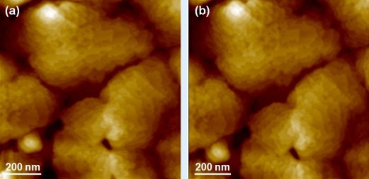
Figure 1. Topography images of pentacenefilm imaged at (a) 1Hz and (b) 10Hz.
Scan size: 1µm × 1µm, image size: 512px× 512px
Nowadays, with Park’s NX series of AFM systems and high frequency cantilevers, one can generate AFM images at the expected high resolution and increased scan speed. All Park NX series AFMs are built for Zscanner feedback speed and optimizedZservo control so that anultra highfrequency cantilever is all that is needed to carry out high-speed AFM imaging. Dubbed Fast Imaging, Park’s solution to the need for expediting AFM image generation enables the operator to perform quick and accurate imaging of sample surfaces that have a variation in feature heights ranging from single nanometers to tens of nanometers.
EXPERIMENTS
The Park NX10 AFM was used to perform a fast imaging operation with the ultra-short cantilevers (USC) supplied by NanoWorld. USC has a spring constant of 3N/m and a resonance frequency of 2MHz. Three commercial products were imaged to test the ease of use and accuracy of the AFM’s fast imaging capability. All experiments were run under non-contact mode using the Park Smart Scan AFM operation software.
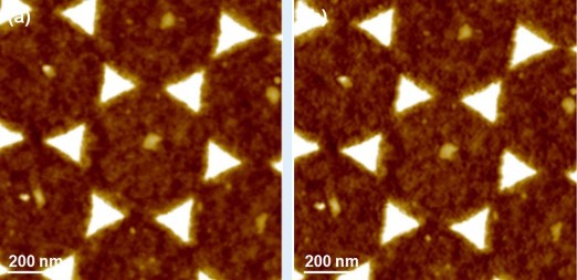
Figure 2. Topography images of triangular aluminum production patterns imaged at (a) 1Hz and (b) 10Hz.
Scan size: 1µm × 1µm, image size: 512px× 512px
In Figure 2, the sharp edges of the 15nm high triangular aluminum production pattern can be clearly revealed at both low and high speed without sacrificing any image quality.
The faster 10 Hz imaging speed allows one to see at a quality equal to the image produced at 1 Hz.
The first sample imaged was Pentacene film. Pentacene is a polycyclic aromatic hydrocarbon consisting of five linearly-fused benzene rings. The rings are connected to form a structure that has surface height differences of roughly 10 nanometers. It is a highly conjugated compound that can be used an organic semiconductor. The second sample that was run was a triangular aluminum production pattern. The third sample tested was Celgard, a material used as a separator and filtration membrane inporous lithium ion batteries as well as in several medical applications. The surface of Celgard has a high variation of feature heights, on the order of tens of nanometers. All samples were imaged with a speed increase from 1Hz to 10 Hz.
RESULTS AND DISCUSSIONS
Combined with the Park SmartScan AFM operation software, fast imaging on the Park NX10 AFM system is as user-friendly as the AFM’s already highly accessible basic non-contact mode. The high productivity, high resolution, and high performance of this technique were well exhibited from the sample measurements to be discussed. As a promising organic semiconductor for film and device applications, Pentacene and the growth of defects and grain boundaries on it are of great interest to researchers. AFM is the main analysis technique to study the characteristics of this material [1]. Figure 1 clearly exhibits the Pentacene surface features such as the holes (defects) and the monolayer structures. With the scanning speed increased from 1Hz (Figure 1a) to 10Hz (Figure 1b), there is no obvious difference between these observed features. We believe with a scanning speed of 10Hz, the changes in the Pentacene’s surface topography can be well tracked in environments that promote real growth or dissolution. Celgard is perhaps the most structurally complex of the three samples scanned with fast imaging. Its structure comes from it being a porous material that is made by stretching isotactic polypropylene [2]. Celgard’s topography is composed of areas with drawn fibrils and areas with undrawn crystalline lamella (Figure 3). Due to the height variation and the fact that the fibrils are freely suspended, the fibrils are very challenging to track for conventional techniques. Figure 3 provides us proof that the details of the surface structure were captured perfectly even at the speed of 10 Hz.
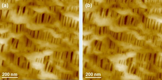
Figure 3. Topography images of Celgard imaged at (a) 1Hz and (b) 10Hz.
Scan size: 1µm × 1µm, image size: 512px× 512px
