Current Trends in Spintronics and NanoStructured Materials
- 26 Sep 2016
- Volume 8
- NanoScientific Magazine, Fall 2016

Aaron Littlejohn is a fourth year Ph.D. student working under Professor GwoChing Wang in the Nanostructure Science Laboratory of Rensselaer Polytechnic Institute’s Department of Physics, Applied Physics and Astronomy. He is a researcher in Rensselaer’s Center for Materials, Devices and Integrated Systems (cMDIS), a multidisciplinary collaboration between scientists and engineers from a variety of fields founded with the ultimate goal of fostering a safe, secure, and sustainable world by making significant contributions to science and technology. His work is supported through Focus Center – New York (FC-NY) as part of a partnership between the state government, leading research institutes, and the U.S. microelectronics, optoelectronics, bioelectronics and telecommunications industries. FC-NY is a founding member of the Interconnect Focus Center (IFC) – a cooperation between universities and the semiconductor research industry – and one of four primary sites along with Massachusetts Institute of Technology, Stanford University and Georgia Institute of Technology.
Aaron’s past research has involved studying the effects of deposition parameters on the electronic and optoelectronic properties of semiconductor alloy films. By slightly altering the growth environment many materials properties can be tuned to serve the needs of a specific application. He also researches the growth of van der Waals heterostructures, or 2D/3D and 3D/2D material combinations. This involves the growth of layered materials on bulk, non-layered substrates and traditional materials on layered substrates, and deviates from conventional heteroepitaxial film growth due to fundamental differences in the bonding mechanisms at the interface. He is currently working on developing new methods for synthesizing layered materials for various applications including solar cells, lithium ion batteries and integrated circuits. One exciting project involves studying the magnetic properties of vanadium disulfide (VS2), a material which shows promise for implementation in next-generation spintronics systems.
Can you explain briefly how you are studying new methods for synthesizing layered materials for various applications including solar cells, lithium ion batteries and integrated circuits and what benefits could result from this research?
Thin to ultrathin layered materials (and all materials in general) can be synthesized by a variety of methods from simple exfoliation – Geim and Novoselov used Scotch tape to thin down carbon to the one monolayer thickness of graphene – to more complicated techniques involving wet chemistry. When not only stoichiometry, but thickness is a crucial factor, synthesis techniques which provide direct and precise control of this parameter must be utilized. We combine well known deposition techniques (thermal deposition, sputtering, e-beam evaporation, etc.) with reactive annealing processes to form transition metal dichalcogenides (TMDCs), for example. The materials we choose to study typically have been shown either experimentally or theoretically by density functional calculations to exhibit interesting and potentially beneficial properties. These properties may insight groundbreaking advances in nanotechnology, electronics or optoelectronics by allowing existing devices to operate more quickly or use less energy, or by serving as the foundation for some new technology that does not yet exist. One of the great things about working in science, is that each discovery could potentially change the world in some unforeseen or unintended way. By characterizing the properties of a new material, we may provide the last puzzle piece to other scientists or engineers working on entirely unrelated projects.
What are the latest research findings regarding the growth of van der Waals heterostructures, or 2D/3D and 3D/2D material combinations?
The study of van der Waals heterostructures is an exciting and highly active area of research at the moment because of its deviations from conventional heteroepitaxy. Layered materials, which exhibit strong in-plane chemical bonds but weak physical bonds between atomic layers can in theory be exfoliated or synthesized in ultrathin form down to just one atom thick. This is highly intriguing for several reasons: 1)The properties of a film in the ultrathin form may be dramatically different than those of the bulk material. This is of fundamental interest in addition to the potential applications; 2)The next generation of electronic devices may be made using ultrathin films, allowing them to be much smaller. This could be beneficial in increasing speed and efficiency while simultaneously using less material to do so. If material costs of production can be reduced, devices will cost less. Devices have already been engineered which use monolayer graphene and molybdenum disulfide (MoS2), to name a couple.
In addition, by utilizing layered materials as the substrates for growth of other materials, one can take advantage of film atoms nucleating ona 2D surface which is free of dangling bonds (unpaired valence electrons). The bonding at the 2D/3D interface is thus much weaker than in traditional epitaxial growth. This allows for the growth of strainfree films without the requirement of lattice matching, a restriction which dramatically limits the choice of substrates in the growth of conventional heterostructures. Without strain at the interface, films grown by van der Waals epitaxy (vdWE) should be high quality with few defects, making them prime candidates for device implementation.
In addition to the study of a variety of 2D/3D and 3D/2D material combinations, recent applications of vdWE involve the growth of nonplanar nanostructures (e.g. nanowire arrays) for use in semiconductor devices. Future research will continue to demonstrate the viability of vdWE as a method for epitaxial film grown and potentially delve into the growth of ultrathin films on ultrathin substrates, taking the trend of scaling down to the next level.
What is methylammonium lead tribromide (MAPbBr3) and how is it being used to create a dramatic reduction in the radiation doses used during medical examination of the human body? Are there any other potential uses for (MAPbBr3) in other applications?
Methylammonium lead tribromide (MAPbBr3) falls under the class of materials known as organoleadtrihalide perovskites (OTPs) which have received much attention lately for use in photovoltaics and radiation detectors. MAPbBr3 specifically has recently been used to fabricate an X-ray detector which is capable of high sensitivity sensing of very low dosesof X-rays [Wei et. al, Nature Photonics 10, 333-340, 2016]. This material attenuates X-ray photons much more efficiently than do materials that are currently used in X-ray detectors. As a result, less of this material is needed to capture X-rays than is needed for others. In addition, the product of charge carrier mobility (μ) and charge carrier lifetime (τ) (or mu-tau (μ-τ) product), which serves as a benchmark for charge collection efficiency is a record high for MAPbBr3, explaining the new detector’s high efficiency and sensitivity. This detector could reduce the intensity of radiation necessary to evaluate the human body during medical examination. The exciting optoelectronic properties of MAPbBr3 may also allow it to be used in high efficiency hybrid perovskite solar cells and environmental gas detectors [Fang et al. Science Advances 2016;2:e1600534].
How do you use Park Atomic Force Microscope in your research and which features to you find the most useful?
The Park XE-7 atomic force microscope is absolutely critical to my research. It allows me to generate 3D reconstructions of sample surfaces to view them with higher magnification than is possible by other microscopy techniques. I use these surface scans to extract quantities for height-height correlation analysis from which I can determine roughness parameters. I am consistently able to achieve sub-nanometer resolution which ensures the accuracy of my data. I use the large range scan mode to collect survey scans measuring as much as hundreds of square microns in area and obtain finer images for quantitative purposes in small scan mode. The precision of the Park AFM’s non-contact mode repeatedly gives scans of the highest quality.
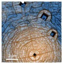
MAPbBr3 film – 10 × 10 μm scan Contours reveal atomic layer step edges of just a couple angstroms in height. Regular features (square trenches and straight lines) formed due to strain relief within the film Square trenches approx. 8 – 10 nm deep ‘Grid lines’ approx. 1 – 2 nm deep.
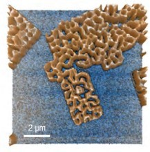
MAPbBr3 film – 10 × 10 μm scan AFM allows us to explore the effects of deposition conditions on growth mechanisms in ultrathin films. This is a region of the same film which we believe was exposed to a slightly different environment (either through exposure to contaminant atoms, or different temperature or pressure). The lighter areas (film) are about 20 nm taller than the blue areas.
Are the nanoscale images created by AFM essential to your current research and why?
The nanoscale images collected using our Park AFM is essential to our current research. They provide a way to examine the morphology of the films grown in our lab which we use to calibrate deposition parameters. Surface roughness is one crucial parameter to measure when characterizing a film. It has major implications to the quality of interfaces at heterojunctions, which plays a large role in device efficiency, for example in solar cells. We can also deduce growth mechanisms, or how the film nucleates and evolves, from a film’s morphology as revealed by AFM. The analysis software also makes it easy to create publication quality figures.
Can you tell us generally how spintronics is changing data storage and the semiconductor industry?
The theoretical foundation of spin-dependent electron transport has only been around for the past couple of decades. Spintronics, short for spintransport electronics, will use electric and magnetic fieldsto manipulate the spin angular momentum of electrons in addition to their charge as a second degree of freedom. Spin adds to the information transmitted in a circuit and can be maintained even without applying power. Thus relative to today’s electronics, spintronic circuits have the potential to exhibit increased data processing speeds and decreased power consumption, making for a revolution in computing ability.This has shaped the research efforts of many industry and academic groups toward finding materials to make next-generation spintronic devices a reality.
What is vanadium disulfide (VS2) and how might the study of the magnetic properties be used in next-generation spintronics systems?
Vanadium disulfide (VS2) is a layered transition metal dichalcogenide (TMDC) comprised of layers of V atoms sandwiched between layers of S atoms. In the past, it has been studied as a potential anode for lithium ion batteries, supercapacitors, and moisture sensors. Because it exhibits a layered structure, it should be possible to exfoliate or to grow VS2 in monolayer form. One major area of research in spintronics is that of finding materials which will be suitable for implementation in spintronic systems. Ultrathin to monolayer VS2 shows promise for use in spintronic devices because of its unique ferromagnetic properties which can be directly manipulated by applying isotropic strain. By increasing strain across the VS2 monolayer from -5% to +5%, the magnetic moments of the atoms within the material increase monotonically [Y. Ma et al. ACS Nano 6, 2, 1695- 1701, 2012]. This unique property could be utilized in many devices including spintronics as a mechanical switch for control of spinpolarized electron transport. However, these properties have only been predicted by density functional calculations – I hope to synthesize and characterize this material’s electronic and magnetic properties to study the calculations’ validity. I’m also working on synthesizing different oxides of vanadium (VO2, V2O5), which show promise due to the tunability of their ferromagnetic properties.

“RELATIVE TO TODAY’S ELECTRONICS, SPINTRONIC CIRCUITS HAVE THE POTENTIAL TO EXHIBIT INCREASED DATA PROCESSING SPEEDS AND DECREASED POWER CONSUMPTION, MAKING FOR A REVOLUTION IN COMPUTING ABILITY. THIS HAS SHAPED THE RESEARCH EFFORTS OF MANY INDUSTRY AND ACADEMIC GROUPS TOWARD FINDING MATERIALS TO MAKE NEXT-GENERATION SPINTRONIC DEVICES A REALITY. ULTRATHIN TO MONOLAYER VS2 SHOWS PROMISE FOR USE IN SPINTRONIC DEVICES BECAUSE OF ITS UNIQUE FERROMAGNETIC PROPERTIES WHICH CAN BE DIRECTLY MANIPULATED BY APPLYING ISOTROPIC STRAIN.”
What advances in spintronics do you see in the future that might have a great impact on society?
Because I’m working on the ground floor of materials synthesis and characterization and not the engineering of said materials into devices, this one is admittedly a bit tough for me to answer…but I can say that the impact of spintronics will be great. Faster, more powerful devices will come in smaller packages at lower cost to manufacturers. This will mean an enhancement in quality and accessibility of our current technology as well as the invention of new technologies which may solve problems currently facing the world and improve our standard of living. It’s impossible to say just how much spintronics will change the world, but the future is certainly exciting.