Scanning Probe Magnetic Microscopy with Magnetoresistive Magnetic Sensors
- 19 May 2026
- Volume 30
- NANOscientific Magazine, 2026
Dr. Aurélie Solignac, SPEC, CEA, CNRS, Université Paris-Saclay, CEA Saclay, France
Introduction
Magnetic imaging at the micro- and nanoscale is an essential tool for investigating magnetic phenomena in materials science, condensed matter physics, and nanotechnology. Beyond fundamental research, spatially resolved magnetic measurements are increasingly important in applied and industrial contexts, including the analysis of electronic circuits, magnetic nanostructures, and sensing components such as magnetic encoders used in microrobotics. In many of these cases, the goal is not only to visualize magnetic structures but to obtain quantitative maps of the magnetic field distribution with high spatial resolution and, ideally, across a broad frequency range in order to obtain more information on the magnetic properties of the material.
Scanning probe magnetic microscopy offers a powerful approach for achieving this objective by measuring the magnetic stray field emitted by a sample with a sensor scanned in close proximity to the surface. Among the various sensing technologies available, magnetoresistive sensors provide a compelling combination of sensitivity, broadband detection capability, and room-temperature operation.
This article is based on a presentation by Dr. Aurélie Solignac at the recent Europe NanoScientific Forum, describing the development of a scanning probe magnetic microscope that integrates giant magnetoresistive (GMR) sensors into flexible cantilevers for quantitative and broadband magnetic field imaging.
Magnetic Microscopy Techniques
A range of techniques is available for imaging magnetic fields at small length scales. Many of these approaches are based on scanning probe methods in which a localized sensor is scanned across the sample surface to measure the magnetic stray field.
Among the most widely used methods is Magnetic Force Microscopy (MFM). In MFM, a magnetized probe tip interacts with the magnetic field gradient above the sample surface. Changes in cantilever dynamics caused by this interaction are used to image the magnetic structure. MFM provides high spatial resolution but the technique is inherently indirect, as it measures force gradients rather than the magnetic field itself. Additionally, the magnetized probe can influence the sample due to the stray field it produces.
Another emerging technique involves nitrogen-vacancy (NV) centers in diamond. NV-based magnetometry uses a quantum defect embedded at the apex of a diamond tip as a magnetic sensor. Radio frequency (RF) excitation and optical readout of the defect allow highly sensitive magnetic measurements with excellent spatial resolution. NV sensors also offer the possibility of vector magnetic field measurements. However, the requirement for ODMR (optical detected magnetic resonance) detection increases experimental complexity and can limit measurement speed.
Scanning SQUID (superconducting quantum interference device) microscopes represent another highly sensitive approach. These systems can detect extremely small magnetic signals, but they generally require cryogenic operation and complex instrumentation.
Between these approaches lies a category of techniques based on Hall sensors and magnetoresistive sensors, which offer a balance between sensitivity, spatial resolution, and experimental simplicity.
One way to compare magnetic microscopy techniques is to examine the trade-off between magnetic field detectivity and spatial resolution. Techniques such as MFM and NV magnetometry provide high spatial resolution but typically lower detectivity. SQUID systems provide exceptional detectivity but with greater operational complexity. Magnetoresistive sensors occupy an intermediate region, combining moderate spatial resolution with robust magnetic sensitivity.
Other practical considerations also influence technique selection. These include the ability to perform quantitative measurements, measurement speed, compatibility with applied magnetic fields, and the possibility of measuring multiple magnetic field components. The potential for the probe itself to perturb the sample must also be considered.
Within this landscape, magnetoresistive sensors offer several advantages, particularly their broadband frequency response and straightforward electrical detection.
Principles of Magnetoresistive Sensing
Magnetoresistive sensors are based on the interaction between electron spin and magnetization in ferromagnetic materials. In such materials, the electrical resistance depends on the relative orientation of electron spin and the magnetization of the material. This effect forms the foundation of spintronics, a field that has transformed magnetic sensing and data storage technologies.
In a giant magnetoresistance (GMR) device, the sensor consists of two ferromagnetic layers separated by a thin spacer layer. The electrical resistance of the structure depends on the relative orientation of the magnetization in these layers. When the magnetizations are parallel, the resistance differs from the case when they are antiparallel.
To achieve stable operation, one of the layers is typically designed as a reference layer, whose magnetization remains fixed. The other layer acts as a free layer, whose magnetization rotates in response to an external magnetic field. Changes in the relative orientation of these layers result in measurable changes in electrical resistance.
Although the simplified concept involves only two magnetic layers separated by a spacer, practical devices use more complex multilayer stacks fabricated by sputtering on silicon substrates. These stacks may incorporate synthetic antiferromagnetic structures that stabilize the reference layer while minimizing stray magnetic fields generated by the sensor.
Magnetoresistive technology has reached a high level of industrial maturity. For more than three decades, GMR and TMR (tunnel magnetoresistance) sensors have been used in the read heads of hard disk drives and remain essential components in modern data storage systems. MR sensors are also widely used in automotive and industrial applications due to their robustness and reliability.

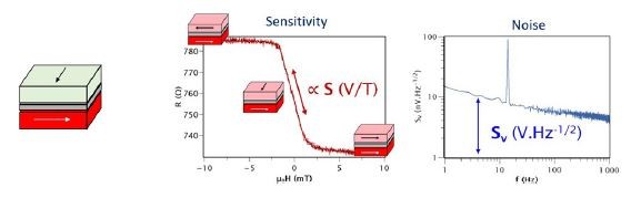
Noise and Detectivity
The detectivity of a magnetic sensor depends on both its sensitivity and its noise characteristics.In magnetoresistive sensors,a significant source of noise at low frequencies is 1/f noise.This Noise Component Dominates Measurements Near Dc,Reducing The Effective Sensitivity Of The Sensor.However,As Measurement Frequency Increases,The Contribution From 1/F Noise Decreases Significantly.As A Result,The Intrinsic Sensitivity Of The Sensor Can Be Fully Utilized At Higher Frequencies.This Property Gives Magnetoresistive Sensors An Important Advantage For Applications That Involve Dynamic Magnetic Signals.Their Ability To Operate Over A Broad Frequency Range Enables Detection Of Both Static And Time-Varying Magnetic Fields.
Integration Into A Scanning Probe System
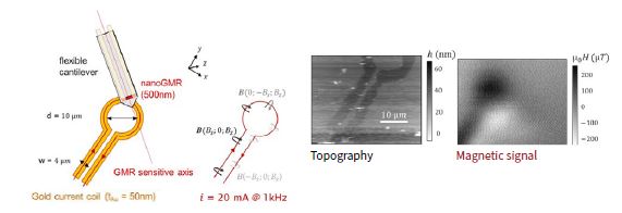
To Use Magnetoresistive Sensors For Magnetic Microscopy,The Sensor Must Be Integrated Into A Probe Capable Of Scanning The Sample Surface.The System Presented At The Nanoscientific Symposium Incorporates The Gmr Sensor Into A Flexible Cantilever Compatible With A Scanning Probe Microscope.
In This Configuration,The Cantilever Performs Two Simultaneous Measurements.The Mechanical Deflection Of The Cantilever Provides Topographic Information,As In Conventional Atomic Force Microscopy.At The Same Time,The Gmr Sensor Detects The Local Magnetic Field Generated By The Sample.
Unlike Conventional Afm Probes,The Design Does Not Rely On A Sharp Tip To Obtain High Magnetic Spatial Resolution.Instead,The Cantilever Is Oriented So That The Magnetoresistive Sensor Itself Is Positioned As Close As Possible To The Sample Surface.The Magnetic Spatial Resolution Of The Measurement Is Therefore Determined Primarily By The Size Of The Sensor And The Sensor–Sample Distance.
An Important Feature Of This Configuration Is The Decoupling Of Topography And Magnetic Signals.The Topographic Measurement Is Obtained From Cantilever Deflection,While The Magnetic Signal Is Measured Electrically Through The Magnetoresistive Sensor.
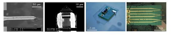
Sensor Fabrication
The Fabrication Of The Scanning Probe Begins With The Deposition Of The Multilayer Magnetoresistive Stack Using Sputtering Techniques.The Stack Is Then Patterned Using Lithographic Processes To Define The Geometry Of The Sensor And To Create Electrical Contacts For Resistance Measurements.
To Improve Spatial Resolution,Nanofabrication Techniques Are Used To Reduce The Lateral Dimensions Of The Magnetoresistive Element.However,Reducing Sensor Size Can Increase Noise Levels,Which May Reduce Detectivity.The Design Process Therefore Involves Balancing Spatial Resolution Against Sensor Performance.
Following Sensor Fabrication,Additional Microfabrication Steps Are Used To Create The Flexible Cantilever Structure Surrounding The Sensor.The Resulting Probe Resembles A Conventional Afm Cantilever But Incorporates The Magnetoresistive Sensing Element Near Its End.
Electrical Connections Are Made Through Wire Bonding To A Printed Circuit Board That Interfaces With The Scanning Probe Microscope Electronics.
Magnetic Imaging Demonstration
The capabilities of the scanning magnetoresistive microscope were demonstrated using a simple test structure consisting of a current loop. When current flows through the loop, it generates a magnetic field that can be detected by the scanning sensor.
Simultaneous measurements of topography and magnetic field were performed during scanning. The resulting images show a clear separation between structural and magnetic information.
After applying basic signal filtering, the measured magnetic field distribution was compared with simulations based on electromagnetic theory. The experimental measurements showed good agreement with the simulated magnetic field, demonstrating that the technique can provide quantitative magnetic field mapping.
Broadband Magnetic Measurements
A particularly notable feature of magnetoresistive sensors is their broadband frequency response. This capability allows magnetic signals originating from different physical phenomena to be separated in the frequency domain.
In the demonstration presented at the NanoScientific Forum, a test sample was designed to illustrate this capability. The sample consisted of a ferromagnetic rectangular structure positioned beneath a current-carrying line. The current in the line was modulated at a frequency of 1 kHz.
During scanning, the magnetoresistive sensor acquired magnetic data over a broad frequency range. Analysis of the signal revealed two distinct contributions. The DC component corresponded to the stray magnetic field produced by the ferromagnetic structure. Meanwhile, the 1 kHz component corresponded to the magnetic field generated by the alternating current in the line.
This example demonstrates how broadband acquisition allows multiple magnetic phenomena to be observed and distinguished within a single measurement.
Outlook
The integration of magnetoresistive sensors into scanning probe cantilevers represents an important step toward versatile magnetic microscopy systems capable of quantitative and broadband measurements.
Future developments may focus on extending the frequency range of measurements to explore dynamic magnetic properties such as magnetic susceptibility.
Additional functionality could also be achieved by incorporating multiple sensors oriented along different directions, enabling measurement of multiple magnetic field components.
Further improvements may involve reducing probe-induced stray fields through optimized sensor structures or exploring alternative magnetoresistive architectures such as tunnel magnetoresistance (TMR) devices.
As magnetoresistive technology continues to advance, its integration with scanning probe microscopy is expected to provide increasingly powerful tools for nanoscale magnetic characterization across both scientific research and industrial applications.

Aurélie Solignac is a researcher at CEA, in the Nanomagnetism and Oxides Laboratory of the Department of Condensed Matter Physics. Her expertise is in the field of electronic spin sensors, magnetic imaging, thin film heterostructures and materials. Following one of the LNO's research axes, she is involved in the development and characterization of magnetoresistive sensors for various applications. She is co-leading the French magnetometry network.

References
PhD Julien Moulin (2019) Paris Saclay University. https://theses.hal.science/tel-02976807v1/file/91585_MOULIN_2020_archivage.pdf