Primer: The Advancements And Applications Of Scanning Spreading Resistance Microscopy (SSRM)
- 12 May 2024
- Volume 26
- NANOscientific Magazine, SPRING 2024
Introduction
To advance the fields of semiconductor device technology and energy storage solutions, various analytical methods have been established. Among these, Scanning Spreading Resistance Microscopy (SSRM) is gaining recognition for its effectiveness in analyzing the electrical properties of semiconductors and batteries. SSRM, operating under the principles of Scanning Probe Microscopy (SPM), employs a tip coated with a conductive material that traverses a surface—be it semiconductor, metal, or battery material—with an applied electrical bias. This innovative approach allows the tip to measure key electrical properties such as current, conductance, and resistance, providing insights into the microscale electrical behaviors of these materials. Particularly noteworthy is SSRM's capacity to use a logarithmic amplifier, enabling the assessment of a broad range of materials from insulators to metals. This capability is pivotal not only in enhancing the performance and reliability of semiconductor devices but also in advancing our understanding of battery materials, contributing to the development of more efficient and durable energy storage systems.
Technical Challenges and Solutions
A common challenge with semiconductor and metal surfaces is that they can form an insulating oxide layer when exposed to the atmosphere. To obtain accurate resistance measurements, SSRM ensures an ohmic (unrestricted) contact by removing this oxide layer, thus allowing direct contact with the underlying material. This is achieved using a robust diamond-coated AFM (Atomic Force Microscopy) tip. For precise measurements, a significant force is applied between the tip and the sample to penetrate any oxide or contamination layer. Moreover, performing SSRM measurements in a controlled environment like a vacuum or under a nitrogen atmosphere is advised to prevent the sample surface from undergoing re-oxidation or moisture adsorption during the analysis process.
SSRM vs. SRP: Comparative Analysis
For the purpose of assessing a wide range of resistances within semiconductor devices, which typically consist of layers of metal, semiconductor, and oxide with resistances spanning from ohms to giga ohms, the use of a logarithmic current amplifier is crucial. This is due to the fact that a linear current amplifier is limited to a small current range determined by its gain setting. Scanning Spreading Resistance Microscopy (SSRM) is a refined adaptation of the traditional Spreading Resistance Profiling (SRP) method, applied at the micro and nanoscale to cross-sectioned samples.
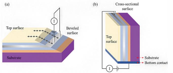
Unlike the conventional SRP that relies on a dual probe system with probes around 1 μm in radius, SSRM employs an AFM tip with a much smaller radius of only a few tens of nanometers, scanning narrowly defined regions of the device. This is depicted in Fig. 1, which contrasts the SRP and SSRM setups. SSRM, avoiding the carrier dispersion issues associated with beveled surfaces in SRP, measures resistance between a back-contact and the AFM tip along a cross-sectional surface. The calculation of resistance follows Ohm's law (R = V/I), with the spatial resolution hinging on the tip's radius of curvature. The precision in resistance measurements relies heavily on minimizing contact resistance, which can be achieved by applying greater force between the tip and the sample. To ensure an optimal Ohmic contact, SSRM requires not only a high contact force but also a contaminant-free sample surface and stable environmental conditions. Accordingly, an AFM probe designed with a stiff lever and a robust tip is recommended to perform accurate SSRM measurements.
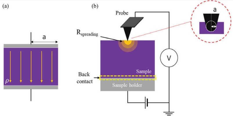
In a typical setting, current flows throughout the entire area of a sample. However, with SSRM, when the sample is engaged with a sharp AFM tip, it allows for the detection of current spread in the immediate vicinity of the tip, due to the small contact area. This is illustrated in Fig. 2(b). The formula for spreading resistance in an ideal scenario is RS = ρ/4a, where ρ represents the local resistivity of the sample and a stands for the contact area, which is influenced by the radius of the AFM tip.
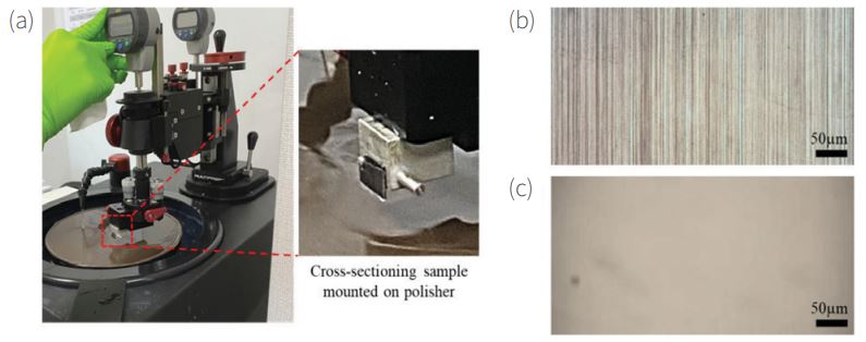
The surface texture of the sample plays a significant role in these measurements. A rough surface can alter the actual contact area between the AFM tip and the sample, complicating the task of obtaining precise resistance values. To counter this, sample preparation through polishing to smooth the surface, followed by cleaning to remove any residue, is essential. This process ensures the acquisition of accurate doping profiles. Fig. 3(a) presents the equipment used for polishing cross-sectional samples, while Fig. 3(b) and Fig. 3(c) depict optical images of sample surfaces, demonstrating the difference between insufficient and sufficient polishing, respectively.
Methodology and Precision in SSRM Measurements
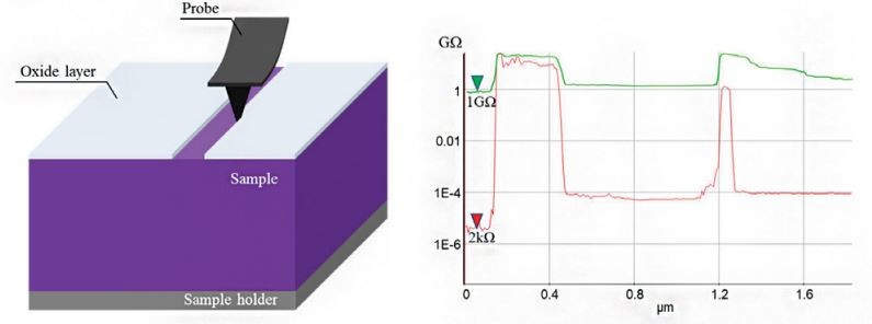
Establishing an ohmic contact between the scanning tip and the sample is crucial in SSRM because the presence of an oxide layer can significantly increase contact resistance. This increase can lead to a Schottky-barrier formation, which would result in inaccurate resistance readings. Fig. 4 illustrates the process of the scanning tip traversing the sample's surface, during which it removes the oxide layer, thereby effectively reducing the contact resistance as shown in Fig. 4(a). The corresponding line profile in Fig. 4(b) displays how the resistance measured at the surface varies in response to different amounts of force applied to the tip.

Case Studies and Applications
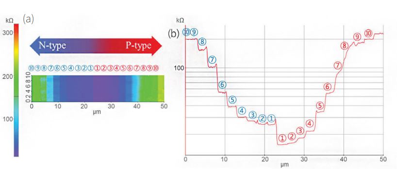
In an experimental demonstration, an IFX dopant calibration sample, known as the "NP20" provided by Infineon, was examined using SSRM with a sample bias of 1.5 V_DC. This particular sample was structured with 20 distinct doping conditions, featuring regions of phosphorus-doped n-type and boron-doped p-type areas on a silicon substrate. The resultant SSRM resistance image, Fig. 5(a), along with the line profile depicted in Fig. 5(b) highlight the variance in resistance across the array of doped states. These variations were captured using a logarithmic current amplifier, which is capable of spanning the entire dynamic resistance range of the sample, from the lowest to the highest resistances presented by the different dopant states.
Conclusion
In summary, Scanning Spreading Resistance Microscopy (SSRM) serves as a vital tool for the precise electrical analysis of semiconductor devices. SSRM's capability to penetrate insulating layers and measure resistance across a broad range of conductivities enhances its utility in the semiconductor industry. Critical factors for its success include the need for a clean sample surface and controlled environmental conditions to ensure accuracy. The technique's application to both semiconductor calibration and lithium-ion battery analysis highlights its versatility and potential impact on the development of advanced electronic materials and energy storage solutions. SSRM thus represents a significant stride forward in nanoscale material characterization.