Utilizing High-Throughput and High-Resolution Automated 3d-AFM For CD Measurement and Trench Sidewall Characterization
- 10 Nov 2025
- Volume 29
- NANOscientific Magazine, 2025
Dr. Nithi Atthi, Thai Microelectronics Center (TMEC), National Science and Technology Development Agency (NSTDA), Thailand
Adapted from Presentation, Edited by NanoScientific
Intro: Precision Metrology for a New Era of Power Devices
At the 2024 NanoScientific Symposium, Dr. Nithi Atthi from the Thai Microelectronics Center (TMEC), an organization under the National Science and Technology Development Agency (NSTDA), Thailand, spotlighted a pivotal transformation underway in the semiconductor industry—one driven by the explosive demand for AIoT devices, electric vehicles, and the next generation of power electronics. Central to this shift is silicon carbide (SiC), a wide bandgap semiconductor rapidly replacing traditional silicon with high-power and high-efficiency devices.
As the industry transitions from planar structures to advanced trench-based architectures for higher voltage ratings—often exceeding 1200 to 3000 volts—the fabrication challenge intensifies. Optimizing trench geometry, minimizing electric field concentration at corners, and ensuring smooth, low-roughness sidewalls have become critical steps for performance and reliability.
This is where advanced metrology becomes essential. Atomic Force Microscopy (AFM), especially in automated 3D configurations, has emerged as a uniquely capable tool to measure critical dimensions (CD), trench profiles, and sidewall roughness at nanoscale resolution—parameters that directly determine device yield, leakage current, and long-term stability and reliability.
Dr. Atthi’s presentation focused on the deployment of fully automated 3D-AFM (Park NX-3DM) for high-throughput, high-accuracy trench characterization from Park Systems in SiC and silicon-based power device applications. His work demonstrates not only the measurement capability but also the process optimization insights that can be extracted from precise 3D profiling.
From Planar to Trench: Why SiC Devices Demand 3D Metrology
Traditional power devices were predominantly fabricated in planar geometries, where the source, gate, and drain regions were defined along a flat surface. While effective for moderate voltages, this design faces limitations as voltage demands escalate for EV inverters, renewable energy systems, and industrial power electronics.
Trench structures—etched vertically into the substrate—allow a shorter channel length and conduction path, reducing current crowding at the surface, lowering on-resistance, and improving channel mobility. SiC in particular enables narrower trench widths to allow tighter cell pitch and higher channel densities in the same area, further increasing performance.
However, these advantages come with engineering challenges. The bottom of the trench, if etched with a sharp radius, can concentrate electric fields, creating premature breakdown points and compromising device lifetime, as shown in Fig. 1. Similarly, excessive sidewall roughness can serve as a leakage pathway. The trench profile—shape, corner radius, and smoothness—must be carefully optimized through etch chemistry and post-processing such as oxidation and annealing.
This demands metrology that can quantify:
• Trench geometry (width, depth, angle)
• Corner curvature at the trench bottom
• Sidewall and bottom roughness at sub-nanometer levels
• Critical dimensions (CD) at top, middle, and bottom of the trench
AFM, especially when configured for sidewall access, is one of the few techniques capable of providing this complete set of measurements with the required resolution.
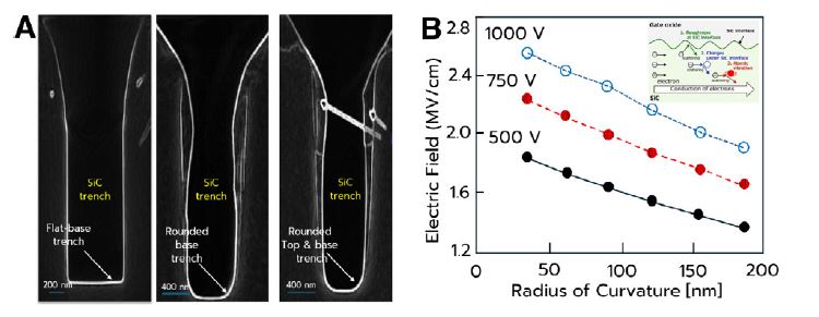
base trench, and rounded top & base trench, and B) effects of radius of curvature of the
bottom of the trench to the electric field of SiC power device.
Automated 3D-AFM: A Metrology Platform for Production
Dr. Atthi introduced the Park NX-3DM, a fully automated AFM system designed for semiconductor production lines. Unlike laboratory AFMs used for research, the NX-3DM integrates with semiconductor fab workflows, supporting 6-inch, 8-inch, and 12-inch wafers with SEMI-standard SMIF or FOUP material handling.
Key features include:
• Automation: Robotic wafer handling, pre-alignment, and recipe-driven measurement sequences.
• Non-contact scanning: Minimizes tip wear and sample damage, critical for repetitive measurements.
• Automatic tip exchange and tuning: Ensures consistent performance and minimizes downtime.
• Tilting scanning head: Allows rotation of the Z-axis to ±19° or ±38° for direct sidewall measurement.
• High aspect ratio tips: Enables probing deep, narrow trenches without profile distortion.
These capabilities make the NX-3DM particularly suited for trench characterization where CD uniformity, profile control, and sidewall roughness all influence device reliability.
Measuring the Sidewalls: Overcoming Conventional AFM Limitations
Conventional AFM excels at measuring flat surfaces, making it suitable for top and bottom roughness measurements. However, sidewalls—especially vertical or near-vertical surfaces and the roughness at the bottom of deep trench structures—are inaccessible to a standard AFM tip scanning in perpendicular approach mode.
The Park NX-3DM addresses this with its tilting head mechanism, allowing the tip to be angled toward the trench sidewalls. By scanning at +19° and -19° tilts, the system captures height data for both the left and right sidewalls. Combined with a normal (0°) scan for top and bottom surfaces, these three datasets are computationally stitched into a full 3D reconstruction of the deep trench structure.
This stitched profile allows precise extraction of:
• Top, middle, and bottom CD values
• Sidewall angles
• Sidewall roughness at specified height intervals (e.g., 20–40% and 60–80% of trench height)
• Corner curvature radius at trench bottom
• Sidewall roughness at the bottom surface of the deep trench
The measurement repeatability is excellent, with depth and CD deviations of less than 1% from design values, and sidewall angle repeatability within 0.3°.
Demonstration: Process Optimization through AFM Data
To illustrate the technique, Dr. Atthi presented a demonstration study on silicon trench structures (SiC wafers being more difficult to procure). The trenches, 2 µm wide in a line-and-space (L/S) pattern and 2 µm deep, were fabricated with oxide hard masks and deep reactive ion etching (DRIE). Post-etch, a series of process steps were applied to smooth the sidewalls:
-
Wet oxidation at 900 °C for 40 minutes in forming gas ambient.
-
Oxide etch-back to remove oxidized roughness peaks.
-
High-temperature annealing for silicon surface flattening in nitrogen at varying temperatures (800 °C, 900 °C, 1000 °C).
-
Additional thin oxide deposition for further smoothing on one sample.
Five samples were prepared with different annealing conditions. Using the NX-3DM, five points across each 6-inch wafer were measured automatically according to a predefined recipe.
The results showed clear trends:
• Pre-flattening sample: Sidewall roughness higher, bottom roughness elevated.
• Annealed at 800 °C: Significant reduction in both sidewall and bottom roughness without changing trench dimensions.
• Higher annealing temperatures: Further smoothing, but diminishing returns.
• Oxide re-deposition: Additional improvement in smoothness.
In the optimized condition, sidewall roughness was reduced to approximately 1 nm (left) and 2.2 nm (right), while preserving trench geometry—critical for electrical performance.
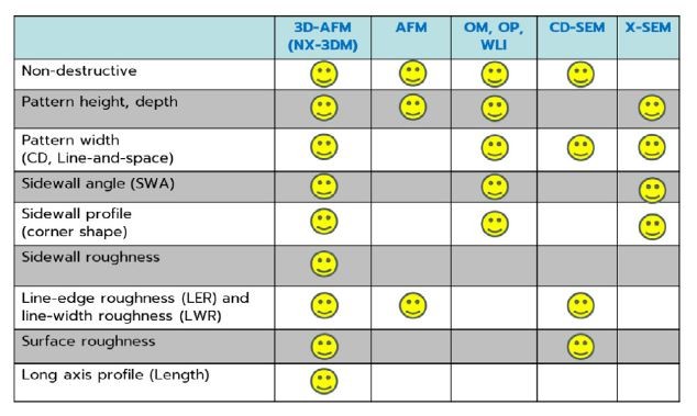
Comparison with Other Techniques
In his talk, Dr. Atthi compared 3D-AFM to other CD and profile measurement methods:
• Critical Dimension–Scanning Electron Microscope (CD-SEM): Good for top-down CD measurement but limited in capturing full sidewall profile and roughness.
• Optical profilers (OP) and white-light interferometers (WLI): Non-contact and fast, but limited by optical resolution and unsuitable for deep, narrow trenches.
• Cross-sectional SEM (X-SEM) and Focused Ion Beam (FIB): Provides profile detail, but destructive and low-throughput.
• Conventional AFM: High resolution for surface roughness, but cannot access sidewalls.
The 3D-AFM offers a non-destructive, high-resolution, full-profile measurement—with automation making it suitable for in-line process control, as shown in Table 1.
Implications for SiC Power Device Manufacturing
The implications for SiC power devices are direct. As Dr. Atthi noted, trench geometry and surface finish are not cosmetic details—they are central to device operation:
• Sharp bottom corners concentrate electric fields, leading to premature breakdown.
• Rough sidewalls create leakage pathways that reduce efficiency and reliability.
• Dimensional variation across wafers can lead to performance spread and yield loss.
By providing detailed, repeatable 3D data on trench structure, automated AFM enables fabs to tune etch and smoothing processes, validate process stability, and catch deviations before they impact production.
Conclusion: Automation Meets Nanoscale Insight
The combination of wide bandgap semiconductors like SiC and advanced trench architectures is reshaping power electronics. But these innovations place unprecedented demands on process control.
Automated 3D-AFM, as demonstrated by Dr. Atthi, offers the precision, repeatability, and throughput needed to meet these demands. By measuring critical dimensions, sidewall roughness, and trench profiles at sub-nanometer precision—non-destructively and across entire wafers—AFM becomes not just a characterization tool, but a process enabler.
As Dr. Atthi concluded, “The fully automated 3D-AFM from Park Systems provides reliable, repeatable, and high-quality data that directly supports the performance and reliability of next-generation power devices.”

Dr. Nithi Atthi is the Fab Manager at the Thai Microelectronics Center (TMEC), part of Thailand’s National Electronics and Computer Technology Center (NECTEC). He holds degrees in Materials Engineering and Engineering Management from Kasetsart University and earned his M.S. and Ph.D. in Electronics and Applied Physics from the Tokyo Institute of Technology under the MEXT Monbukagakusho scholarship.
Dr. Atthi is a recipient of several international fellowships, including Green Talent (Germany), HOPE Meeting (Japan), STS Forum Young Leader (Japan), and the UK’s Leaders in Innovation Fellowship. He has authored over 45 journal publications, delivered more than 122 academic talks, and holds 27 patents.
His research spans wafer fab design, semiconductor process integration (FinFETs, GAA-FETs, MEMS), advanced lithography, and functional surfaces.
References
-
J. Wei, et al., "Review on the Reliability Mechanisms of SiC Power MOSFETs: A Comparison Between Planar-Gate and Trench-Gate Structures," IEEE Transactions on Power Electronics, 38(7), pp. 8990–9005, 2023. DOI: 10.1109/TPEL.2023.3265864
-
Yoo, S. B.; Yun, S. H.; Jo, A. J.; et al. “Automated Measurement and Analysis of Sidewall Roughness Using Three-Dimensional Atomic Force Microscopy,” Applied Microscopy, 52(1), 2022. https://doi.org/10.1186/s42649-022-00070-5
-
Rohm Co., Ltd. “New 4th Gen SiC MOSFETs.” [Online]. Available: https://www.rohm.com/news-detail?news-title=new-4th-gen-sic-mosfets&defaultGroupId=false
Category